Display panel
- Summary
- Abstract
- Description
- Claims
- Application Information
AI Technical Summary
Benefits of technology
Problems solved by technology
Method used
Image

Examples
first embodiment
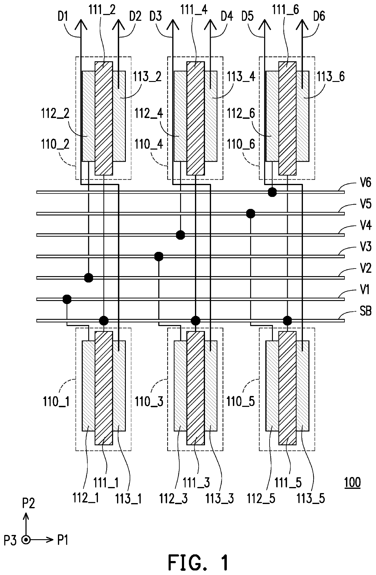
[0022]FIG. 1 is a schematic view of a testing circuit according to the disclosure. Referring to FIG. 1, a circuit 100 includes a testing circuit and a plurality of signal lines D1 to D6. The circuit 100 is a partial circuit of a peripheral region (surrounding area) on a substrate of the display panel. In the present embodiment, the testing circuit includes a plurality of transistors 110_1 to 110_6 electrically connected to the signal lines D1 to D6, and includes a plurality of testing signal lines V1 to V6 and a control line SB. In the present embodiment, the transistors 110_1 to 110_6 are disposed in two groups, which may be divided into an odd group (the transistors 110_1, 110_3, and 110_5) and an even group (the transistors 110_2, 110_4, and 110_6). The two groups of transistors are respectively arranged in a first direction P1 (horizontal direction), and the two groups of transistors are disposed in two rows in a second direction P2 (vertical direction). The first direction P1, ...
second embodiment
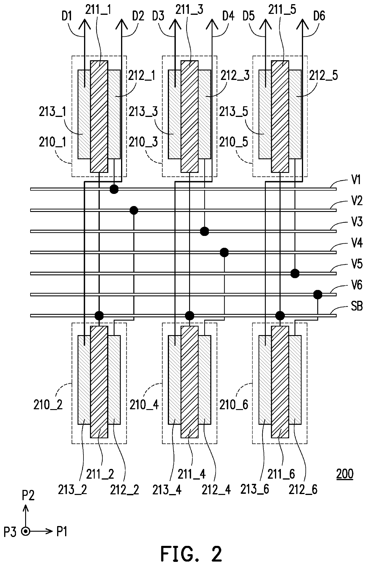
[0027]FIG. 2 is a schematic view of a testing circuit according to the disclosure. Referring to FIG. 2, a circuit 200 includes a testing circuit and a plurality of signal lines D1 to D6. The testing circuit of the present embodiment includes a plurality of transistors 210_1 to 210_6, a plurality of testing signal lines V1 to V6, and a control line SB. The plurality of transistors 210_1 to 210_6 are electrically connected to the signal lines D1 to D6. In the present embodiment, the transistors 210_1 to 210_6 are disposed in two groups, which may be divided into an odd group (the transistors 210_1, 210_3, and 210_5) and an even group (the transistors 210_2, 210_4, and 210_6). The two groups of transistors are respectively arranged in a first direction P1 (horizontal direction), and the two groups of transistors are disposed in two rows in a second direction P2 (vertical direction). The two groups of transistors are separately disposed on both sides of a wire region of the testing sign...
third embodiment
[0036]FIG. 5 is a schematic view of a testing circuit according to the disclosure. Referring to FIG. 5, a circuit 500 includes a testing circuit and a plurality of signal lines D1 to D6. The testing circuit of the present embodiment includes a plurality of transistors 510_1 to 510_6 electrically connected to the signal lines D1 to D6, and includes a plurality of testing signal lines V1 to V6 and control lines SB1 and SB2. In the present embodiment, the transistors 510_1 to 510_6 are disposed in two groups, which may be divided into an odd group (the transistors 510_1, 510_3, and 510_5) and an even group (the transistors 510_2, 510_4, and 510_6). The two groups of transistors are respectively arranged in a first direction P1 (horizontal direction), and the two groups of transistors are disposed in two rows in a second direction P2 (vertical direction). The two groups of transistors are separately disposed on both sides of a wire region of the testing signal lines V1 to V6. In additio...
PUM
 Abstract
Description
Claims
Application Information
 - Generate Ideas
- Intellectual Property
- Life Sciences
- Materials
- Tech Scout
- Unparalleled Data Quality
- Higher Quality Content
- 60% Fewer Hallucinations
Browse by: Latest US Patents, China's latest patents, Technical Efficacy Thesaurus, Application Domain, Technology Topic, Popular Technical Reports.
© 2025 PatSnap. All rights reserved.Legal|Privacy policy|Modern Slavery Act Transparency Statement|Sitemap|About US| Contact US: help@patsnap.com