Light emitting diode package structure

Active Publication Date: 2021-12-23
LITE ON OPTO TECH (CHANGZHOU) CO LTD
View PDF0 Cites 0 Cited by
  • Summary
  • Abstract
  • Description
  • Claims
  • Application Information

AI Technical Summary

Benefits of technology

The patent text describes a new LED package structure that improves the efficiency of the LED. This is achieved by designing the structure so that the top reflecting surface is higher than the input surface and lower than the output surface. This means that more light is reflected and directed out of the LED, resulting in a brighter output.

Problems solved by technology

Accordingly, the luminous efficiency of the LED package structure is negatively affected, and a yellow-ring phenomenon occurs easily.
Referring to FIG. 13, differences of light intensities at different angles of the conventional LED package structure are great; that is, a light uniformity of the conventional LED package structure is poor.
Therefore, the LED package structure shown in FIG. 14 also has problems of poor luminous efficiency and the yellow-ring phenomenon.

Method used


Image

  • Light emitting diode package structure
  • Light emitting diode package structure
  • Light emitting diode package structure

Examples


first embodiment

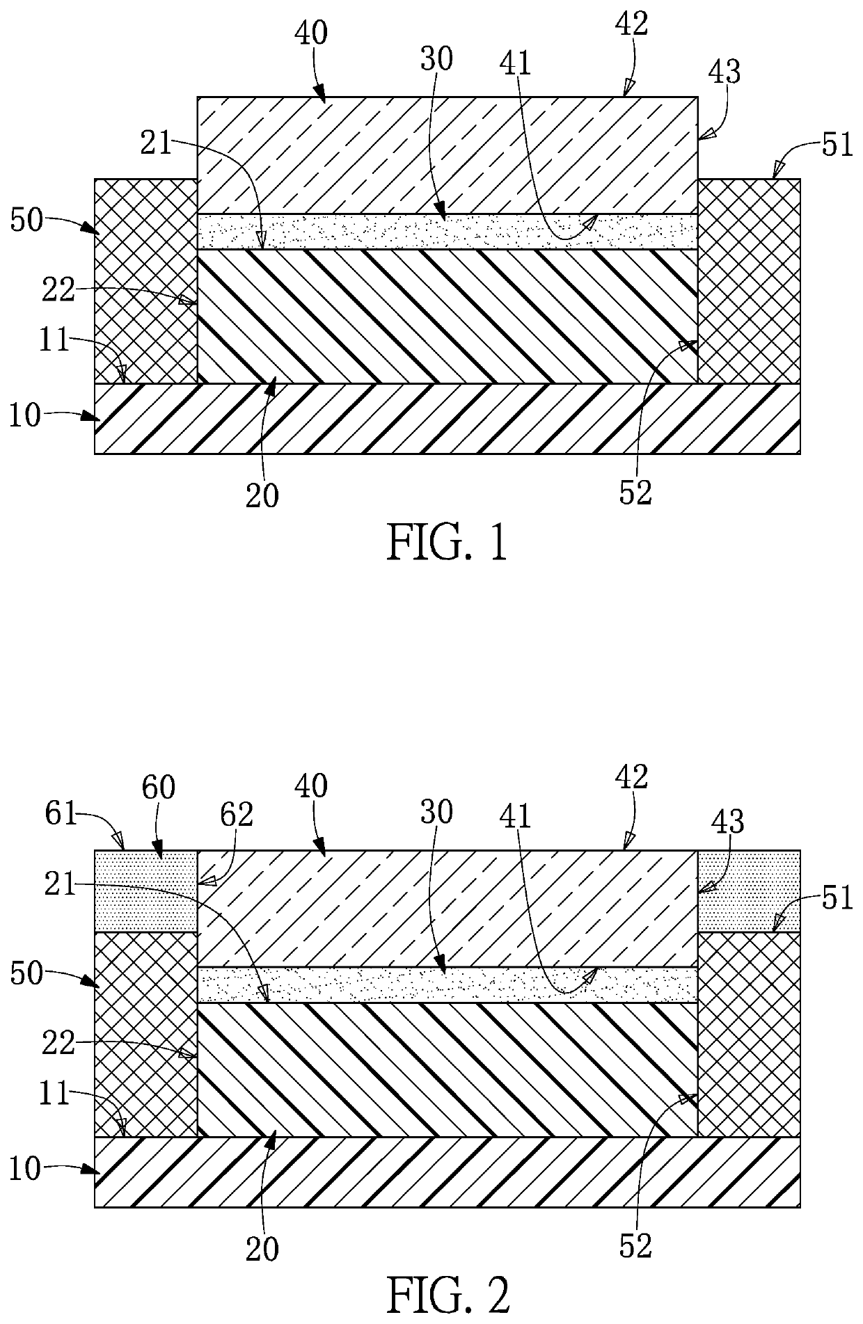
[0056]Referring to FIG. 1, a shape of the light input surface 41 of the wavelength conversion layer 40 corresponds to a shape of the light emitting surface 21 of the light emitting unit 20. In addition, an area of the light input surface 41 is equal to an area of the light emitting surface 21. In the first embodiment, the adhesive layer 30 is disposed between the light emitting unit 20 and the wavelength conversion layer 40.

[0057]The top reflecting surface 51 of the reflective structure 50 is located at a position higher than that of the light input surface 41 and is located at a position lower than that of the top light output surface 42. Accordingly, the light generated by the light emitting unit 20 can be dispersed from the side light output surface 43 of the wavelength conversion layer 40 so that the luminous efficiency of the LED package structure can be enhanced and the yellow-ring phenomenon can be reduced.

[0058]In the first embodiment, the top reflecting surface 51 of the re...

second embodiment

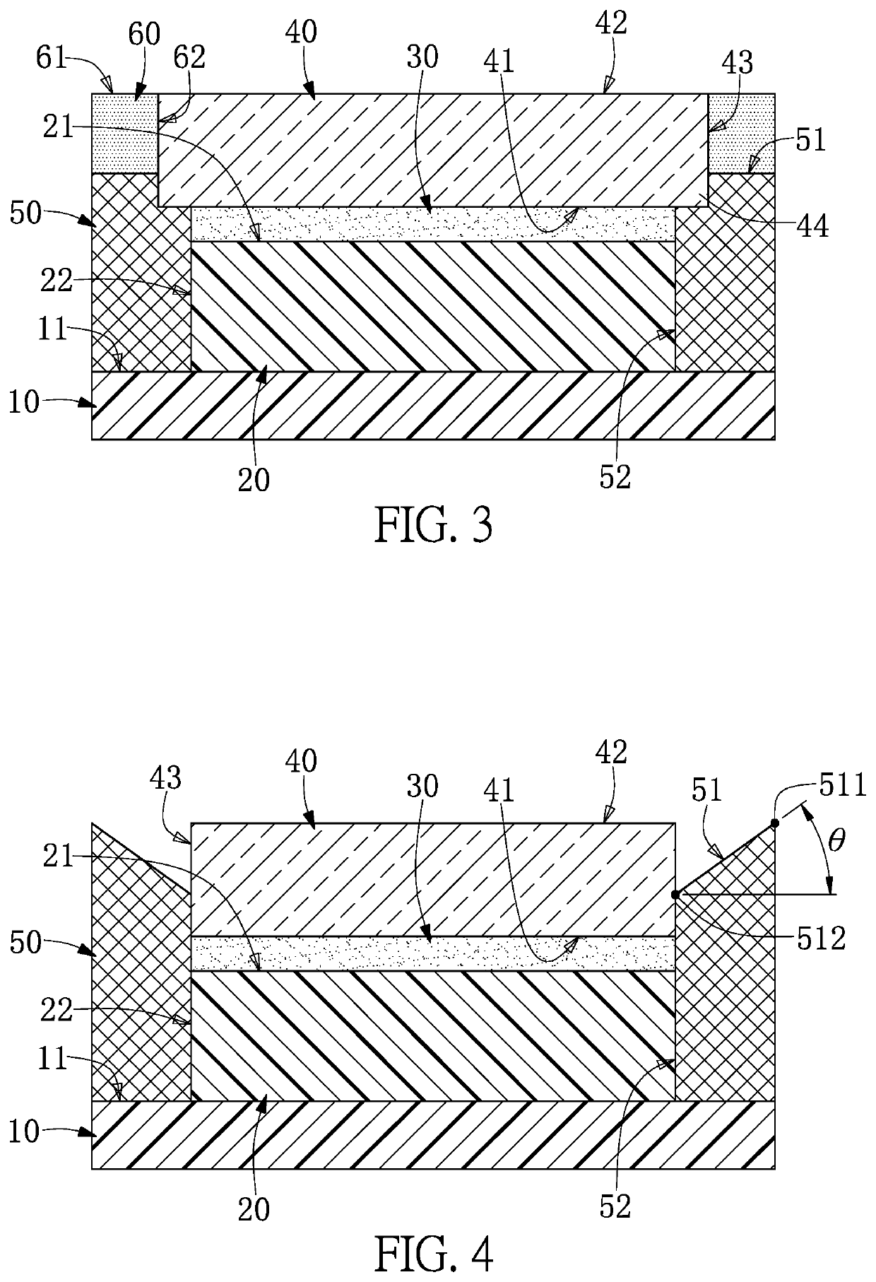
[0061]Referring to FIG. 2, the LED package structure of the second embodiment is similar to the LED package structure of the first embodiment. The difference is that the LED package structure of the second embodiment further includes a light-permeable body 60. The light-permeable body 60 is disposed on the top reflecting surface 51 of the reflective structure 50 and contacts the side light output surface 43 of the wavelength conversion layer 40. Specifically, a concave region is formed between the top reflecting surface 51 of the reflective structure 50 and the side light output surface 43 of the wavelength conversion layer 40. The light-permeable body 60 is filled in the concave region.

[0062]A material of the light-permeable body 60 includes a silicone resin or an epoxy resin. A refractive index of the light-permeable body 60 ranges between a refractive index of the wavelength conversion layer 40 and a refractive index of the air. Accordingly, the light can be converged by the ligh...

third embodiment

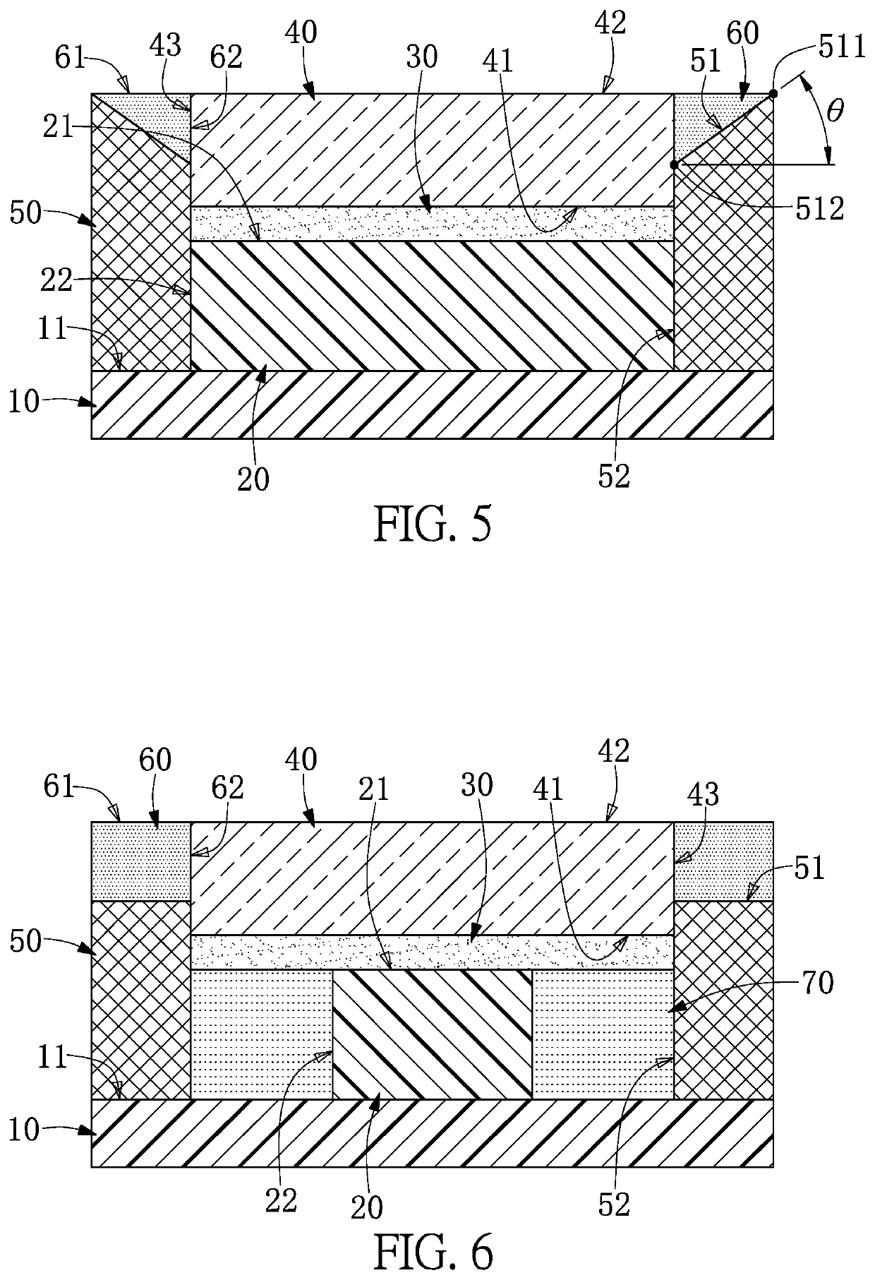
[0064]Referring to FIG. 3, the LED package structure of the third embodiment is similar to the LED package structure of the second embodiment. The difference is that the area of the light input surface 41 of the wavelength conversion layer 40 is larger than the area of the light emitting surface 21 of the light emitting unit 20, so that an illumination area of the LED package structure can be enlarged and the luminous efficiency of the LED package structure can be enhanced.

[0065]Specifically, the light emitting surface 21 of the light emitting unit 20 is completely covered by the light input surface 41 of the wavelength conversion layer 40. An outer end 44 of the wavelength conversion layer 40 is limited in position on the reflective structure 50. In other words, a retaining groove is concavely formed at a junction extending from the top reflecting surface 51 and the inner reflecting surface 52 of the reflective structure 50. The outer end 44 is located at a junction between the lig...


PUM


Abstract

A light emitting diode package structure includes a substrate, a light emitting unit, a wavelength conversion layer, and a reflective structure. The light emitting unit and the reflective structure are disposed on a mounting surface of the substrate. The wavelength conversion layer is disposed on the light emitting unit. The wavelength conversion layer has a light input surface, a top light output surface opposite to the light input surface, and a side light output surface connecting the light input surface and the top light output surface. The reflective structure surrounds the light emitting unit and the wavelength conversion layer. The reflective structure has a top reflecting surface located on a top of the reflective structure, and a height position of the top reflecting surface is higher than a height position of the light input surface and lower than a height position of the top light output surface.

Description

CROSS-REFERENCE TO RELATED PATENT APPLICATION[0001]This application claims the benefit of priority to China Patent Application No. 202010561361.9, filed on Jun. 18, 2020 in People's Republic of China. The entire content of the above identified application is incorporated herein by reference.[0002]Some references, which may include patents, patent applications and various publications, may be cited and discussed in the description of this disclosure. The citation and / or discussion of such references is provided merely to clarify the description of the present disclosure and is not an admission that any such reference is “prior art” to the disclosure described herein. All references cited and discussed in this specification are incorporated herein by reference in their entireties and to the same extent as if each reference was individually incorporated by reference.FIELD OF THE DISCLOSURE[0003]The present disclosure relates to a package structure, and more particularly to a light emit...

Claims


Application Information

Patent Timeline
IPC IPC(8): H01L33/48H01L33/10H01L33/50
CPCH01L33/486H01L33/50H01L33/10H01L33/48H01L33/60F21S41/141F21S43/14F21W2107/10F21Y2115/10H01L33/505H01L33/46
Inventor JIA, SHU-YONGLI, ABNERZHANG, LI
Owner LITE ON OPTO TECH (CHANGZHOU) CO LTD
Why Eureka
Try Eureka