Packaging structure of light emitting diode

Inactive Publication Date: 2009-11-26
LO WEI HUNG
View PDF7 Cites 6 Cited by
  • Summary
  • Abstract
  • Description
  • Claims
  • Application Information

AI Technical Summary

Benefits of technology

[0007]One objective of the present invention is to provide a light-emitting diode (LED) packaging structure which employs two materials with differ

Problems solved by technology

The inadequate design of the luminescent angle of the LEDs shown in FIGS. 1 and 2

Method used


Image

  • Packaging structure of light emitting diode
  • Packaging structure of light emitting diode
  • Packaging structure of light emitting diode

Examples


Example

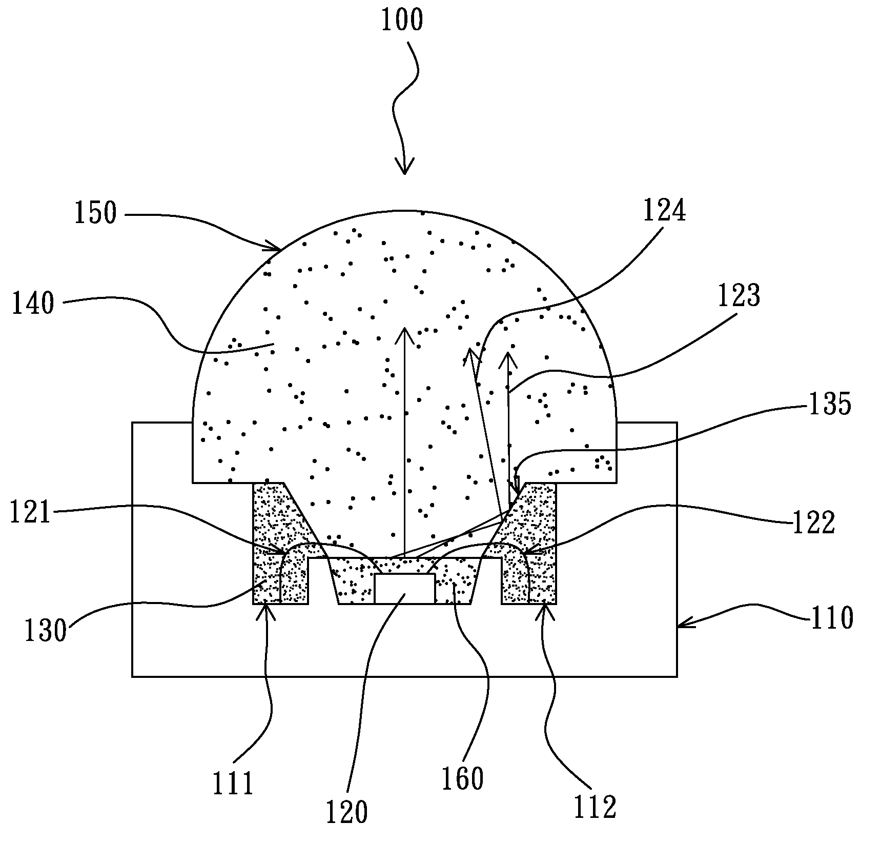
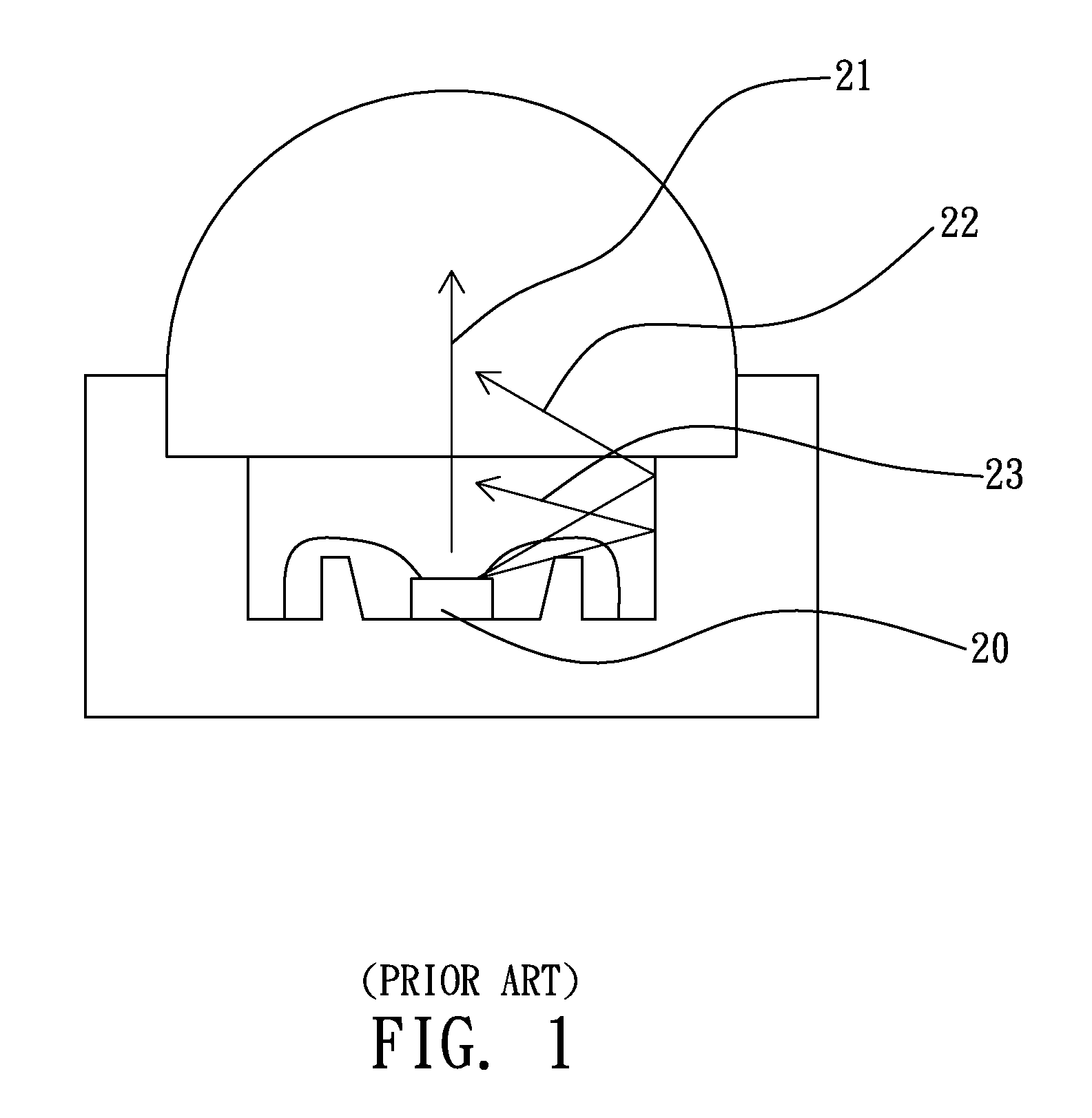
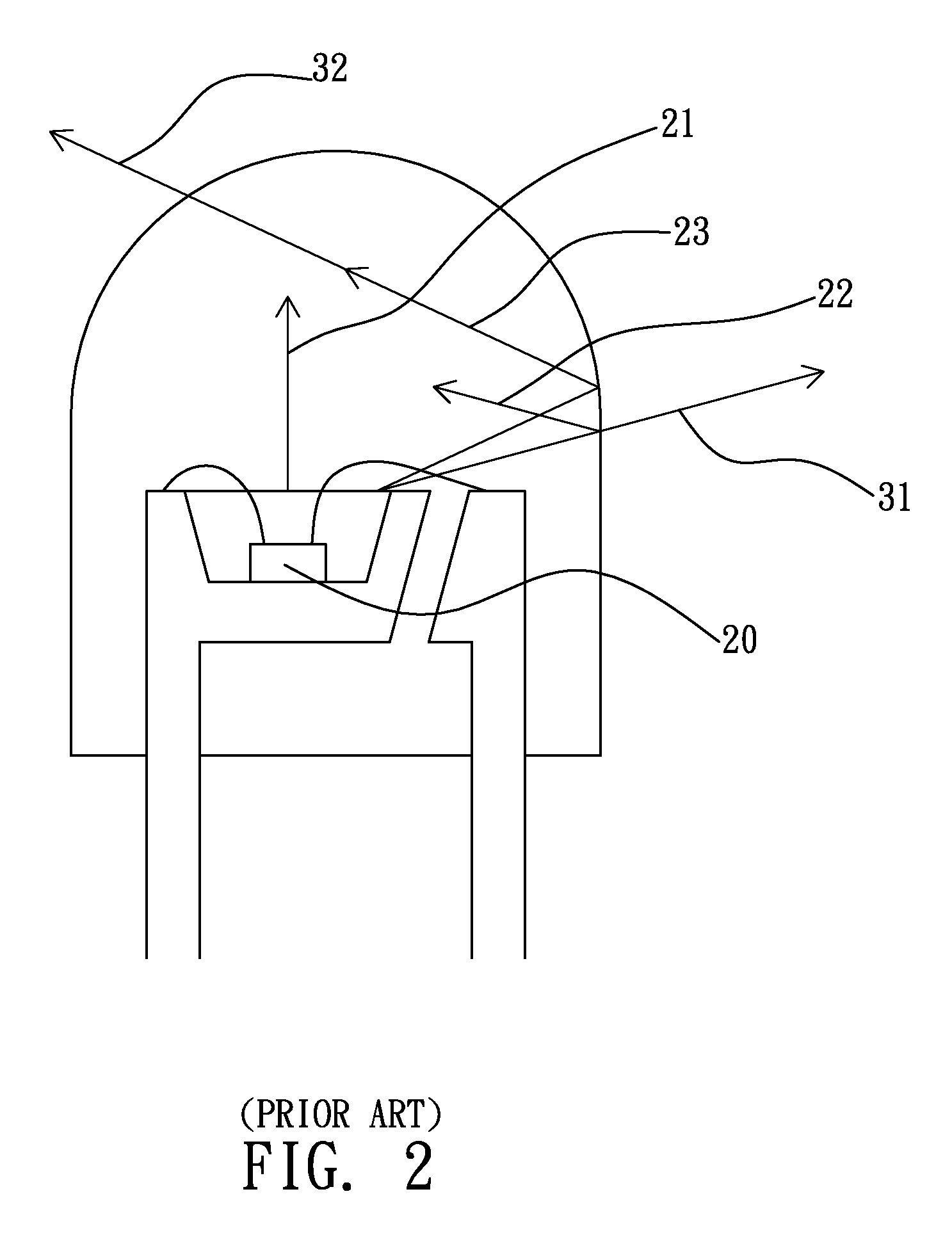
[0015]FIG. 3 illustrates the cross-sectional view of a light-emitted diode (LED) packaging structure according to the present invention.

[0016]With reference to FIG. 3, a LED packaging structure 100 according to the present invention is, for example but not limited to, a surface-mount LED, comprising a base 110, a chip 120, a first materials 130, a second material 140, and a ball lens 150.

[0017]The base 110 is disposed with a positive connection pad 111 and a negative connection pad 112 to be coupled with a printed circuit board (not shown). The base 110 is conventional art of a LED packaging structure. It is not the focus of the present invention and therefore will not be discussed hereafter.

[0018]The chip 120 is disposed upon the base 110 and coupled with the positive connection pad 111 and the negative connection pad 112 with two conducting wires 121 and 122, respectively, wherein the chip 120 may emit required electroluminescent light of different colors, which is a conventional ...


PUM


Abstract

The present invention discloses a light-emitting diode packaging structure, comprising a base; a chip; a first material disposed on at least one side of the chip and having a first refraction index; a second material disposed upon the chip, having a second refraction index, and separated with the first material with an interface therebetween to refract the light refracted from the first material; and a ball lens disposed upon the second material and forming a confined space with the base; whereby, the light emitted from the chip refracts through the first refraction material and the second refraction material and finally emits out from the ball lens.

Description

FIELD OF THE INVENTION[0001]The present invention relates to a light-emitting diode packaging structure, and in particular to a light-emitting diode packaging structure which can enhance the luminescent efficiency of light-emitting diodes.BACKGROUND OF THE INVENTION[0002]The modern light-emitting diode (LED) industry has been striving to enhance LED's luminescent efficiency, which is determined by the following factors: (1) the luminescent efficiency of LED chip, including the internal efficiency which involves transforming internal electric energy into light energy in the LED chip, and the external efficiency which involves the light emitted from the chip interior to its exterior; (2) the light conversion efficiency of phosphor (if necessary); for example, the most common commercial white LED packaging structure employing blue light chip and yellow phosphor; and (3) the design of packaging structure, most of which stresses the choice of transparent materials, such as high light tra...

Claims


Application Information

Patent Timeline
IPC IPC(8): H01L33/00H01L33/56H01L33/58
CPCH01L33/58H01L33/56H01L2224/48091H01L2224/48247H01L2224/48257H01L2224/8592H01L2924/181H01L2924/00014H01L2924/00012
Inventor NAUM, SOSHCHINLO, WEI-HUNGTSAI, CHI RUEI
Owner LO WEI HUNG
Why Eureka
Try Eureka