
Eureka
For R&D, Eureka makes reading and utilizing patents & technical documents easy.
Eureka AIR
Designed for self-driven R&D workflows. Generate viable solutions, solve complex R&D challenges, empower your innovation with AI.

Eureka Materials
Designed for material experts only. Revolutionize your material R&D, from search, analyze, to developing new materials.

TechResearch
Generate reliable direction feasibility study reports for your R&D in just a few steps.

TechSeek
Discover and master advanced knowledge NOW. Basics, ideas, possibilities, all at once.

TechMind
As an expert in R&D Theories, TechMind can generates customized viable solutions instantly.

TechRisk
Analyze your overall solution with one click, know your potential R&D risks in advance.

TechMonitor
Get weekly tech updates, stay abreast of the latest tech innovations and key insights.
Probe card testing device
- Summary
- Abstract
- Description
- Claims
- Application Information
AI Technical Summary
Benefits of technology
Problems solved by technology
Method used
Image

Examples
Embodiment Construction
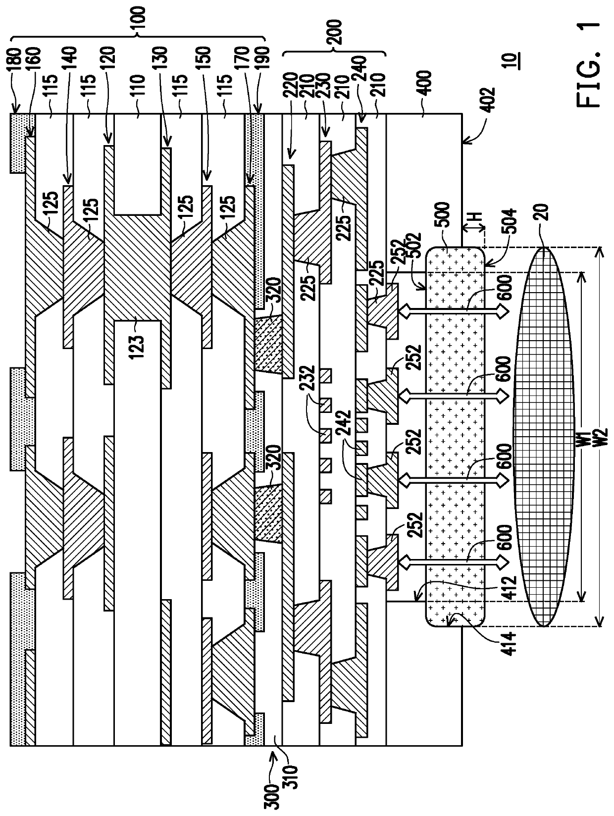
[0023]FIG. 1 is a schematic cross-sectional view of a probe card testing device according to an embodiment of the disclosure. Referring to FIG. 1, in the embodiment, a probe card testing device 10 includes a first sub-circuit board 100, a second sub-circuit board 200, a connecting structure layer 300, a fixing plate 400, a probe head 500, and multiple conductive probes 600. The second sub-circuit board 200 is disposed on one side of the first sub-circuit board 100. The connecting structure layer 300 is disposed between the first sub-circuit board 100 and the second sub-circuit board 200, and the first sub-circuit board 100 is electrically connected to the second sub-circuit board 200 through the connecting structure layer 300. That is, it requires no solder and primer to connect the first sub-circuit board 100 and the second sub-circuit board; and without the use of solder, the bonding yield of the first sub-circuit board 100, the second sub-circuit board 200, and the connecting str...
PUM
 Abstract
Description
Claims
Application Information
 - R&D Engineer
- R&D Manager
- IP Professional
- Industry Leading Data Capabilities
- Powerful AI technology
- Patent DNA Extraction
Browse by: Latest US Patents, China's latest patents, Technical Efficacy Thesaurus, Application Domain, Technology Topic, Popular Technical Reports.
© 2024 PatSnap. All rights reserved.Legal|Privacy policy|Modern Slavery Act Transparency Statement|Sitemap|About US| Contact US: help@patsnap.com