Electronic device

a technology of electronic devices and lasers, applied in the direction of lasers, laser details, semiconductor lasers, etc., to achieve the effect of effectively improving on the problems associated

Pending Publication Date: 2022-04-14
LITE ON TECH CORP
View PDF0 Cites 0 Cited by
  • Summary
  • Abstract
  • Description
  • Claims
  • Application Information

AI Technical Summary

Benefits of technology

[0006]In response to the above-referenced technical inadequacy, the present disclosure provides an...

Problems solved by technology

However, during a manufacturing process of the conventional electronic device, a fixing agent used to fix the components o...

Method used


Image

  • Electronic device
  • Electronic device
  • Electronic device

Examples


first embodiment

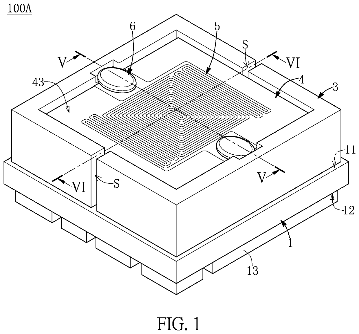
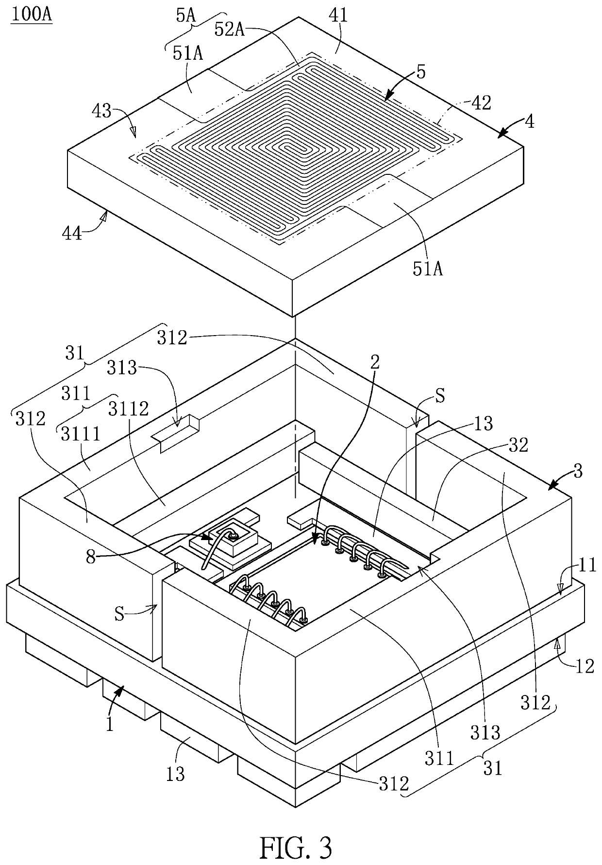
[0040]Referring to FIG. 1 to FIG. 6, a first embodiment of the present disclosure provides an electronic device 100A. Referring to FIG. 1 to FIG. 3, the electronic device 100A includes a substrate 1, a semiconductor unit mounted on the substrate 1, a wall 3 disposed on the substrate 1 and surrounded the semiconductor unit, a light-transmitting member 4 disposed on the wall 3 and covered on the semiconductor unit, a detection circuit 5 formed on the light-transmitting member 4, and an electrically conductive agent 6 that can be electrically coupled to the detection circuit 5 and the wall 3. The following description describes the structure and connection relationship of each component of the electronic device 100A.

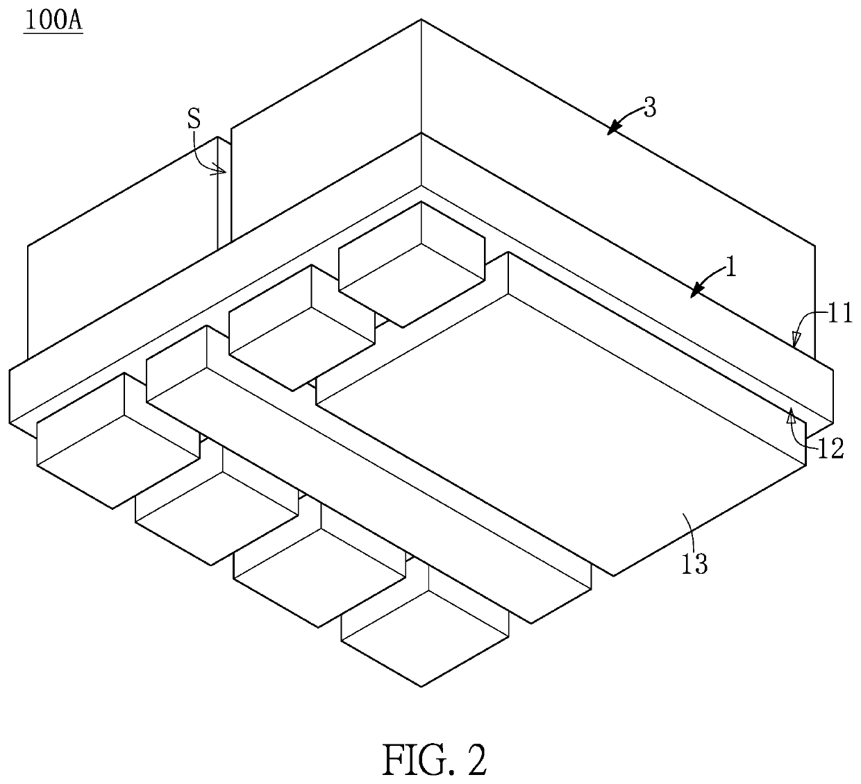
[0041]Referring to FIG. 1 to FIG. 3, the substrate 1 in the present embodiment is substantially in a rectangular shape (e.g., a square or a rectangle) and has a first surface 11 and a second surface 12 that is opposite to the first surface 11. The substrate 1 in the present...

second embodiment

[0068]Referring to FIG. 7 to FIG. 10, a second embodiment of the present disclosure provides an electronic device 100B. The electronic device 100B of the present embodiment is similar to the electronic device 100A of the first embodiment, and the similarities between the present embodiment and the first embodiment will not be repeated herein. The difference between the present embodiment and the first embodiment mainly resides in that the light-transmitting member 4 is supported by the two second steps 3112, and the detection circuit 5 in the present embodiment is an inner detection circuit 5B that can be electrically coupled to the substrate 1 through the two interior wall components 32.

[0069]Referring to FIG. 7 and FIG. 8, specifically, the detection circuit 5 in the present embodiment is formed on the inner surface 44 of the light-transmitting member 4. That is to say, the detection circuit 5 is located inside the electronic device 100B, so that the detection circuit 5 can also b...

third embodiment

[0074]Referring to FIG. 11, a third embodiment of the present disclosure provides an electronic device 100C. The electronic device 100C of the present embodiment is similar to the electronic device 100B of the second embodiment, and the similarities between the present embodiment and the second embodiment will not be repeated herein. The difference between the present embodiment and the second embodiment mainly resides in that the light-transmitting member 4 is supported by the two second steps 3112 and the two interior wall components 32.

[0075]Specifically, the height of each of the two interior wall components 32 relative to the substrate 1 is equal to the height of each of the two second steps 3112 relative to the substrate 1, and the top surface of each of the two interior wall components 32 has a groove 321 formed thereon for receiving a part of the electrically conductive agent 6, and another part of the electrically conductive agent 6 overflows on the two junctions 51B, so th...


PUM


Abstract

An electronic device is provided. The electronic device includes a substrate, a semiconductor unit, a wall, and a light-transmitting member. The semiconductor unit is mounted on the substrate. The wall is disposed on the substrate and surrounds the semiconductor unit. The wall includes two exterior wall components and two interior wall components. The two exterior wall components are spaced apart from each other, so that two gaps are formed between the two exterior wall components. The two gaps are in spatial communication with an installation area that is surrounded by the two exterior wall components. The two interior wall components are arranged in the installation area and spaced apart from each other. The two interior wall components correspond in position to the two gaps and respectively shade parts of the two gaps. The light-transmitting member is disposed on the wall and covered on the semiconductor unit.

Description

CROSS-REFERENCE TO RELATED PATENT APPLICATION[0001]This application claims the benefit of priority to China Patent Application No. 202110919154.0, filed on Aug. 11, 2021 in People's Republic of China. The entire content of the above identified application is incorporated herein by reference.[0002]This application claims priority to the U.S. Provisional Patent Application Ser. No. 63 / 089,296 filed on Oct. 8, 2020, which application is incorporated herein by reference in its entirety.[0003]Some references, which may include patents, patent applications and various publications, may be cited and discussed in the description of this disclosure. The citation and / or discussion of such references is provided merely to clarify the description of the present disclosure and is not an admission that any such reference is “prior art” to the disclosure described herein. All references cited and discussed in this specification are incorporated herein by reference in their entireties and to the sa...

Claims


Application Information

Patent Timeline
IPC IPC(8): H01S5/02257H01S5/02218H01S5/00
CPCH01S5/02257H01S5/183H01S5/0014H01S5/02218H01S5/0683H01S5/02345H01S5/02208
Inventor TSAI, HSIN-WEIYANG, SHU-HUA
Owner LITE ON TECH CORP
Why Eureka
Try Eureka