
Electroluminescence Display Apparatus

a technology of display apparatus and electroluminescence, which is applied in the direction of instruments, static indicating devices, etc., can solve the problems of luminance deviation between regions, low accuracy of compensation, and increase of chip cost, and achieve the effect of reducing image quality deviation

Pending Publication Date: 2022-06-09
LG DISPLAY CO LTD
View PDF0 Cites 0 Cited by
  • Summary
  • Abstract
  • Description
  • Claims
  • Application Information

AI Technical Summary

Benefits of technology

The present disclosure provides an electroluminescence display apparatus that reduces image quality deviation caused by IR drop occurring in a high level driving voltage power line. This means that the apparatus helps to improve the display's image quality. Additionally, it also reduces luminance deviation caused by a ripple deviation of an initialization voltage occurring between a region including a notch and a region including no notch. This means that the apparatus helps to make the display brighter and more uniform.

Problems solved by technology

Technology for predicting IR drop to perform compensation on the basis of a data voltage may be considered for reducing an image quality deviation between pixels, but because such compensation technology is based on prediction, the accuracy of compensation is low and the chip cost increases.
In a screen of each electroluminescence display apparatus, there is a problem where a luminance deviation between a region including a notch and a region including no notch occurs.

Method used


Image

  • Electroluminescence Display Apparatus
  • Electroluminescence Display Apparatus
  • Electroluminescence Display Apparatus

Examples


first embodiment

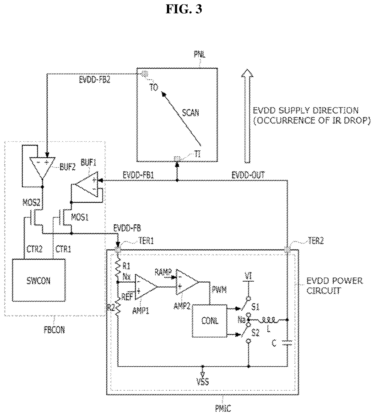
[0066]FIG. 3 is a diagram illustrating a compensation system according to a first embodiment of an electroluminescence display apparatus. FIG. 4 is a diagram illustrating a driving timing of the compensation system according to the first embodiment. FIG. 5 is a diagram for describing a compensation operation of an EVDD power circuit in the compensation system according to the first embodiment.

[0067]Referring to FIGS. 3 and 4, the compensation system according to the first embodiment may include a display panel PNL, an EVDD power circuit, and a feedback control circuit FBCON.

[0068]A plurality of pixels connected to a first power line may be included in the display panel PNL, and each of the pixels may be supplied with a high level driving voltage EVDD-OUT through the first power line.

[0069]The EVDD power circuit may convert a final feedback driving voltage EVDD-FB input through a first input terminal TER1 to output the high level driving voltage EVDD-OUT to a first position TI of the...

second embodiment

[0083]FIG. 6 is a diagram illustrating a compensation system according to a second embodiment of an electroluminescence display apparatus. FIG. 7 is a diagram illustrating a driving timing of the compensation system according to the second embodiment.

[0084]Referring to FIG. 6, the compensation system according to the second embodiment may include a display panel PNL, an EVDD power circuit, and a feedback control circuit FBCON.

[0085]The display panel PNL and the EVDD power circuit of FIG. 6 may be substantially the same as descriptions given above with reference to FIG. 3. However, in terms of a configuration of the feedback control circuit FBCON, FIG. 6 may have a difference with FIG. 3. That is, MOS transistors MOS1 and MOS2 included in the feedback control circuit FBCON of FIG. 6 may be implemented as different channel types, and thus, the MOS transistors MOS1 and MOS2 may be controlled according to one output control signal CTR and a control signal generating circuit SWCON genera...

third embodiment

[0092]FIG. 8 is a diagram illustrating a compensation system according to a third embodiment of an electroluminescence display apparatus.

[0093]Referring to FIG. 8, the compensation system according to the third embodiment may include a display panel PNL, an EVDD power circuit, and a feedback control circuit FBCON.

[0094]The display panel PNL and the EVDD power circuit of FIG. 8 may be substantially the same as descriptions given above with reference to FIG. 3. However, in terms of a configuration of the feedback control circuit FBCON, FIG. 8 may have a difference with FIG. 3. That is, FIG. 8 may have a difference with FIG. 3 in that the feedback control circuit FBCON of FIG. 8 is implemented with thin film transistors TFT1 and TFT2, the thin film transistors TFT1 and TFT2 are provided in the display panel PNL, and separate buffers are not needed. The feedback control circuit FBCON of FIG. 8 may have an advantage where an area mounted on a control board is reduced compared to FIG. 3.

[...


PUM


Abstract

An electroluminescence display apparatus includes a display panel including a plurality of pixels connected to a first power line, a power circuit converting a final feedback driving voltage input through a first input terminal thereof to output a high level driving voltage to a first position of the first power line through a first output terminal thereof, and a feedback control circuit receiving the high level driving voltage as a first feedback driving voltage, receiving a second feedback driving voltage from a second position of the first power line, and supplying the first input terminal of the power circuit with the final feedback driving voltage adjusted based on a first output contribution rate of the first feedback driving voltage and a second output contribution rate of the second feedback driving voltage.

Description

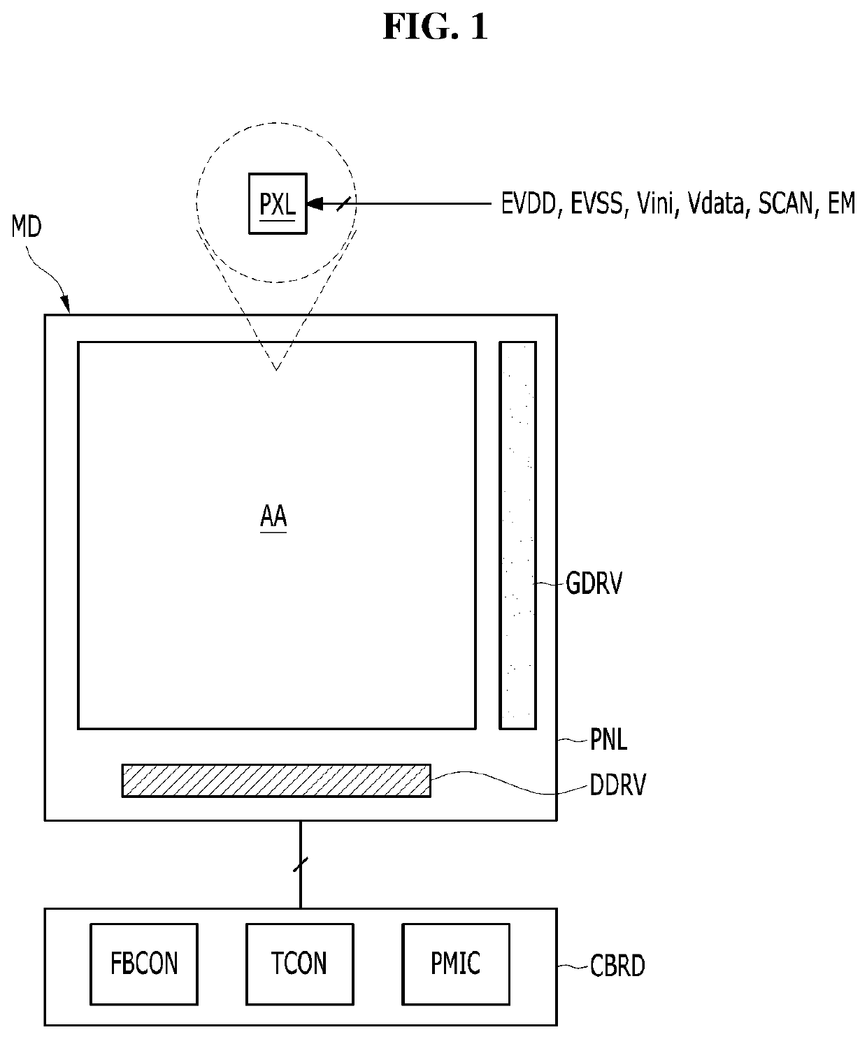
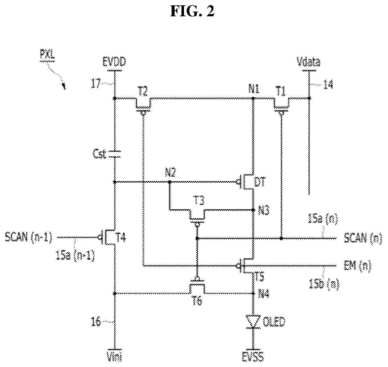
[0001]This application claims the benefit of Republic of Korea Patent Application No. 10-2020-0170583, filed on Dec. 8, 2020, which is hereby incorporated by reference in its entirety.BACKGROUNDField of the Technology[0002]The present disclosure relates to an electroluminescence display apparatus.Discussion of the Related Art[0003]Electroluminescence display apparatuses include a plurality of pixels arranged as a matrix type, and a light emitting device included in each of the pixels emits light on the basis of image data to display luminance. To this end, each pixel may be supplied with a high level driving voltage and an initialization voltage.[0004]Due to dynamic voltage (IR) drop occurring in a power line, a level of a high level driving voltage applied to a pixel varies based on a pixel position, causing an image quality deviation (i.e., a luminance deviation and a color deviation) between pixels.[0005]Technology for predicting IR drop to perform compensation on the basis of a ...

Claims


Application Information

Patent Timeline
IPC IPC(8): G09G3/32
CPCG09G3/32G09G2310/0291G09G2300/0842G09G2330/025G09G2310/08G09G3/3225G09G3/3233G09G2300/0819G09G2300/0861G09G2320/0238G09G2320/0233G09G2320/0242G09G2320/0223G09G2330/028
Inventor KWON, YONG CHULKIM, JUNG JAEKO, NAM KONPARK, DONG WON
Owner LG DISPLAY CO LTD
Learn More