Wire bonding apparatus, method for manufacture of semiconductor device, and semiconductor device

Pending Publication Date: 2022-06-30
SHINKAWA CO LTD
View PDF0 Cites 0 Cited by
  • Summary
  • Abstract
  • Description
  • Claims
  • Application Information

AI Technical Summary

Benefits of technology

The present patent text describes a wire bonding apparatus, method for manufacturing a semiconductor device, and semiconductor device. The invention scrapes the column part using the capillary, and presses down the wire part overlapping the pressure bonded ball using the capillary. This reduces the loop height. Therefore, the technical effects of the invention are to improve the efficiency and reliability of semiconductor device manufacturing.

Problems solved by technology

In many low looping technologies in the related art, since looping is performed in a state in which a column part remains on a pressure bonded ball as it stands, it is difficult to sufficiently reduce the loop height.

Method used


Image

  • Wire bonding apparatus, method for manufacture of semiconductor device, and semiconductor device
  • Wire bonding apparatus, method for manufacture of semiconductor device, and semiconductor device
  • Wire bonding apparatus, method for manufacture of semiconductor device, and semiconductor device

Examples


Embodiment Construction

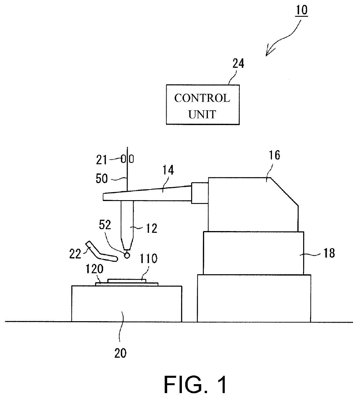
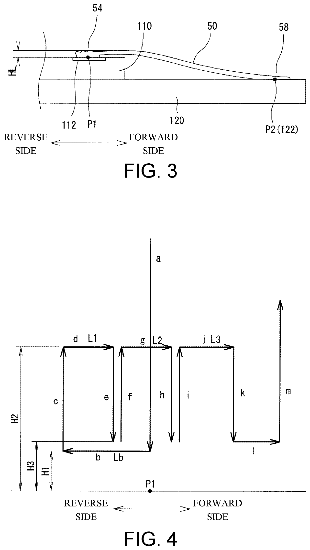
[0034]Hereinafter, a constitution of a wire bonding apparatus 10 will be described with reference to the drawings. FIG. 1 is a view illustrating a constitution of the wire bonding apparatus 10. This wire bonding apparatus 10 is a device connecting a first bonding point P1 and a second bonding point P2 to each other with a wire 50. Generally, the first bonding point P1 is set on a pad 112 of a semiconductor chip 110, and the second bonding point P2 is set on a lead 122 of a lead frame 120 having the semiconductor chip 110 mounted thereon.

[0035]The wire bonding apparatus 10 includes a bonding head 16 and a stage 20 on which the lead frame 120 having the semiconductor chip 110 mounted thereon (both will hereinafter be collectively referred to as “a mounted body”) is placed. The bonding head 16 further includes a bonding arm 14 which functions as an ultrasonic horn and a capillary 12 which is attached to a tip of the said bonding arm 14. The bonding arm 14 is an arm protruding from the ...


PUM


Abstract

This wire bonding apparatus has a capillary, a movement mechanism moving the capillary, and a control unit controlling driving of the movement mechanism. The control unit at least causes execution of: a first process (trajectory a) of lowering the capillary, after a FAB is formed, to pressure bonding height at a first bonding point to form a pressure bonded ball and a column part at the first bonding point; a second process (trajectory b) of moving the capillary horizontally at the pressure bonding height after execution of the first process to scarp off the column part by the capillary; and a third process (trajectory c-k) of repeating a pressing operation at least once after execution of the second process, the pressing operation involving moving the capillary forward and lowering the capillary temporarily during movement so that the capillary presses down on a wire portion positioned over the pressure bonded ball.

Description

TECHNICAL FIELD[0001]The present specification discloses a wire bonding apparatus for connecting a first bonding point and a second bonding point provided on a mounted body to each other with a wire, a method for manufacture of a semiconductor device, and a semiconductor device.BACKGROUND ART[0002]In recent years, in accordance with increase in the level of functionality of portable information terminals, digital AV instruments, IC cards, and the like, mounted semiconductor chips have been required to be smaller and thinner and have a higher level of integration. Particularly, in stack memory devices or the like, memory capacities thereof are determined depending on the number of chips which can be laminated. For this reason, it is important to be able to laminate a larger number of semiconductor chips within a prescribed package height. In order to satisfy such a demand, it is necessary to restrict the heights of wire loops formed through wire bonding. Hence, in the related art, ma...

Claims


Application Information

Patent Timeline
IPC IPC(8): H01L23/00
CPCH01L24/78H01L24/48H01L24/85H01L2224/48096H01L2224/4807H01L2224/48245H01L2224/85986H01L2224/48465H01L2224/78353H01L2224/78303H01L2224/786H01L2224/78824H01L2224/85091H01L2224/48453H01L2224/85181H01L2224/85045H01L2224/78301H01L2224/48451H01L2224/45144H01L2224/45015H01L2224/4809H01L2924/00014H01L24/45H01L2224/85205H01L2924/20751H01L2924/20752H01L2224/05599
Inventor YOSHINO, HIROAKITEI, SHINSUKE
Owner SHINKAWA CO LTD
Why Eureka
Try Eureka