DEADTIME OPTIMIZATION FOR GaN HALF-BRIDGE AND FULL-BRIDGE SWITCH TOPOLOGIES

a switch topology and optimization technology, applied in the direction of power electronics conversion, power conversion systems, climate sustainability, etc., can solve the problems of switching different, dv/dt characteristics, and auxiliary winding voltage sensing,

Active Publication Date: 2022-06-30
GAN SYST
View PDF1 Cites 0 Cited by
  • Summary
  • Abstract
  • Description
  • Claims
  • Application Information

AI Technical Summary

Benefits of technology

[0012]The present invention seeks to provide a method and a circuit for deadtime optimization for half-bridge and full-bridge switch topologies comprising GaN transistors, which mitigate or overcome one or more of the above-mentioned issues, or at least provide an alternative solution.
[0018]For example, the deadtime adjust signal may be used to reduce or optimize deadtime to reduce deadtime losses, while avoiding cross-conduction. If cross-conduction is occurring, the current charge output will be significantly greater than the reference current charge Coss, and the deadtime adjust signal can be used to increase deadtime, or other operating parameters, can be changed, to avoid cross-conduction. If cross-conduction is not occurring, the current charge output will be close to, or ideally will match, the reference current charge Coss. For example, if there is no cross-conduction, the deadtime adjust signal may be used to decrease the deadtime, to reduce deadtime losses, until the current charge output exceeds the reference current charge Coss. Thus, the deadtime can be optimized, e.g. minimized, to a value that avoids cross-conduction, while minimizing deadtime losses.

Problems solved by technology

Disadvantage: requires auxiliary winding voltage sensing.
Disadvantage: The dV / dt characteristics of Si MOSFET switches are different from the dV / dt characteristics of GaN switches; dV / dt detectors designed for Si devices do not work for GaN devices; also, dVDS / dt is non-linear and changes with gate resistance Rg, drain current ID and junction temperature Tj.

Method used


Image

  • DEADTIME OPTIMIZATION FOR GaN HALF-BRIDGE AND FULL-BRIDGE SWITCH TOPOLOGIES
  • DEADTIME OPTIMIZATION FOR GaN HALF-BRIDGE AND FULL-BRIDGE SWITCH TOPOLOGIES
  • DEADTIME OPTIMIZATION FOR GaN HALF-BRIDGE AND FULL-BRIDGE SWITCH TOPOLOGIES

Examples


Embodiment Construction

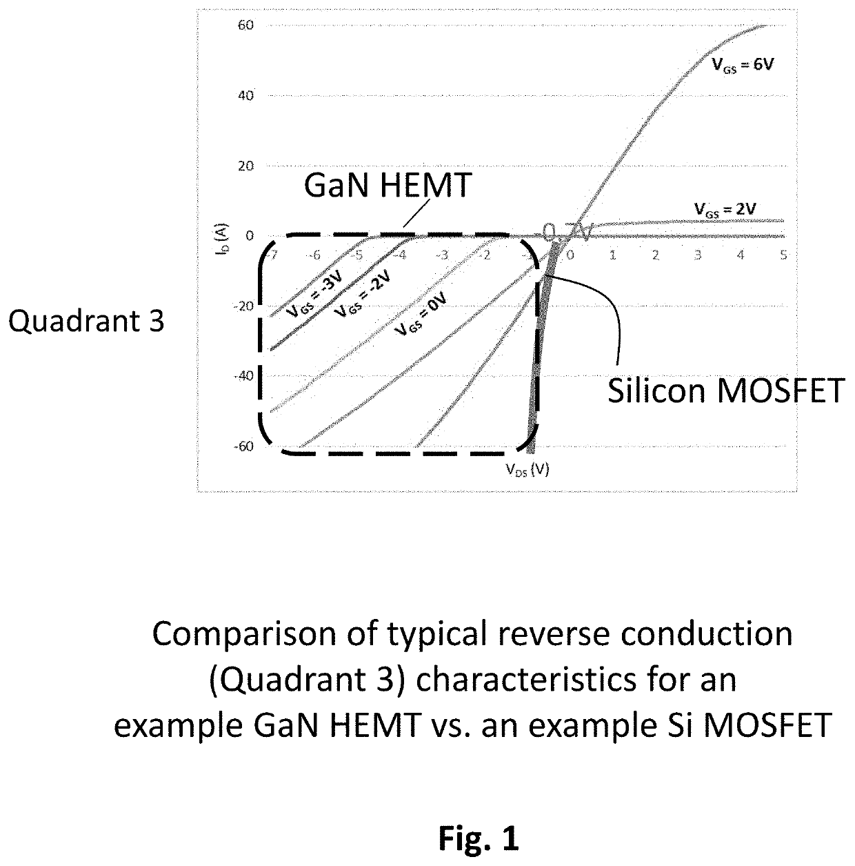
[0038]FIG. 1 shows a comparison of typical reverse conduction (Quadrant 3) characteristics for an example GaN E-HEMT vs. an example Si MOSFET. The reverse conduction of a GaN E-HEMT has a “diode” like characteristic and its reverse conduction voltage drop is higher than for a Si MOSFET, so complementary driving signals are required for driving GaN transistors for half-bridge and full-bridge applications, such as, synchronous rectifiers, buck converters, LLC, ACF and motor drives. A method for deadtime optimization is required for GaN half-bridge and full-bridge switch topologies to avoid cross-conduction while minimising deadtime loss, i.e. minimizing the time of operation in Quadrant 3.

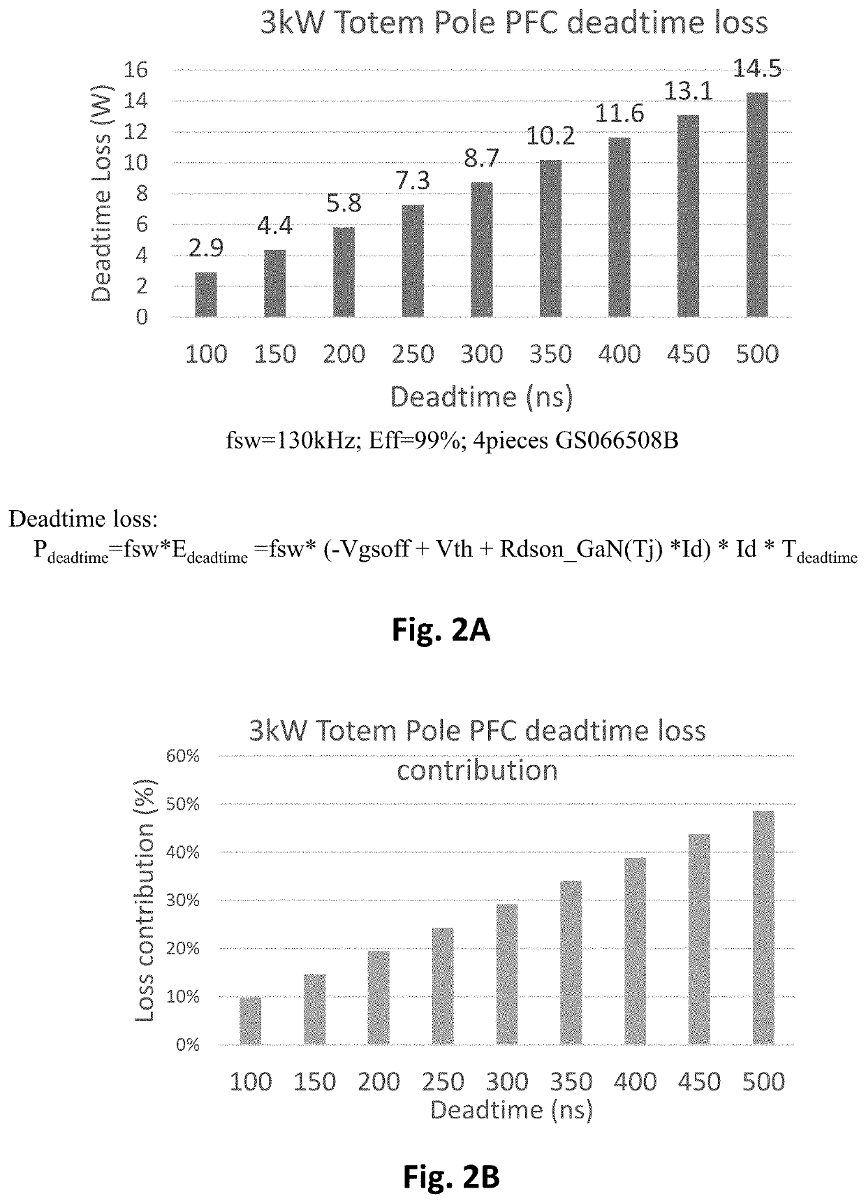
[0039]FIG. 2A shows a plot of Deadtime Loss (W) vs. Deadtime (ns) for an example 3 kW Totem Pole PFC, for a switching frequency fsw=130 kHz. FIG. 2B shows a plot of Deadtime Loss contribution (%) vs. Deadtime (ns) for the example 3 kW Totem Pole PFC.

[0040]The deadtime loss is calculated as:

Pdeadtime=...


PUM

PropertyMeasurementUnit
drain currentaaaaaaaaaa
voltageaaaaaaaaaa
timeaaaaaaaaaa

Abstract

Disclosed is a method for deadtime optimization in a half-bridge switch or full-bridge switch wherein high-side and low-side switches comprise GaN transistors; a circuit for implementing the method; and a power switching system comprising a GaN half-bridge or a GaN full-bridge and a deadtime optimization system. The circuit comprises a drain current bump filter for generating a current charge output; and circuit elements for comparing the current charge output to a reference current charge Coss and generating a deadtime adjust signal. The deadtime adjust signal may be used to adjust deadtime to reduce or minimize deadtime, and deadtime losses, while avoiding cross-conduction.

Description

CROSS-REFERENCE TO RELATED APPLICATION(S)[0001]This application claims priority from U.S. provisional patent application no. 63 / 131,867 entitled “DEADTIME OPTIMIZATION FOR GaN HALF-BRIDGE AND FULL-BRIDGE SWITCH TOPOLOGIES” filed Dec. 30, 2020, which is incorporated herein by reference in its entirety.TECHNICAL FIELD[0002]This invention relates to a power switching devices, such as half-bridge and full-bridge topologies, comprising GaN transistors, e.g. GaN HEMTs (High Electron Mobility Transistors) and methods for deadtime optimization.BACKGROUND[0003]Complementary driving signals are required in half-bridge / full-bridge GaN power switching applications to achieve synchronous rectifying, bidirectional current control, et al. Deadtime is embedded intentionally between the high-side and low-side driving signals to avoid cross-conduction. Deadtime losses becomes non-negligible at high switching frequency. Accurate deadtime control helps to avoid potential cross-conduction while minimizi...

Claims


Application Information

Patent Timeline
Patent Type & Authority Applications(United States)
IPC IPC(8): H02M1/38
CPCH02M1/38H02M1/385Y02B70/10
Inventor QIU, YAJIESPAZIANI, LARRY
Owner GAN SYST
Why Eureka
Try Eureka