Module
a module and module technology, applied in the field of modules, can solve problems such as insufficient shielding performan
- Summary
- Abstract
- Description
- Claims
- Application Information
AI Technical Summary
Benefits of technology
Problems solved by technology
Method used
Image
Examples
first embodiment
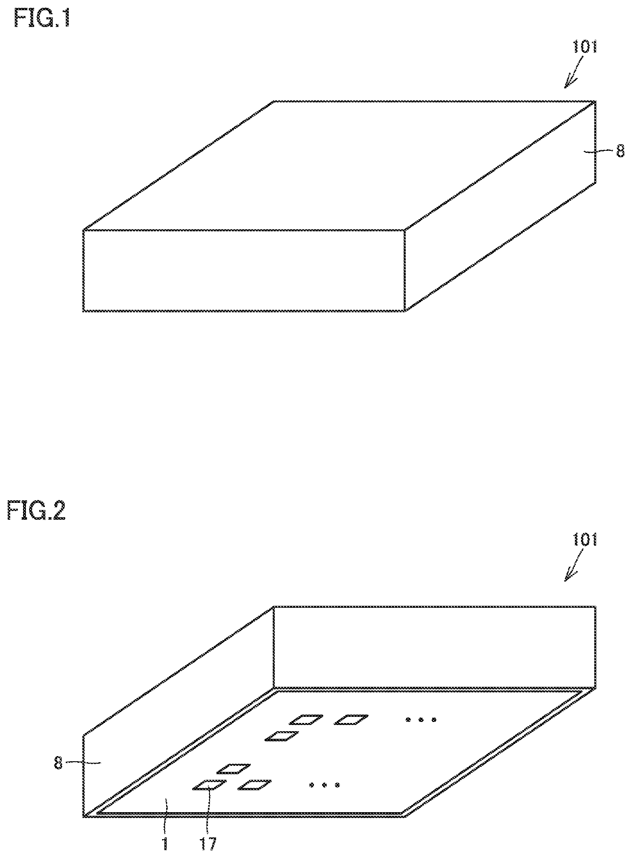
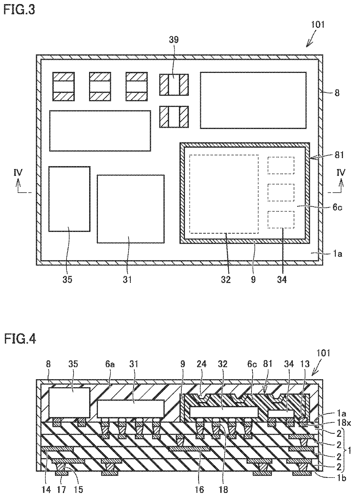
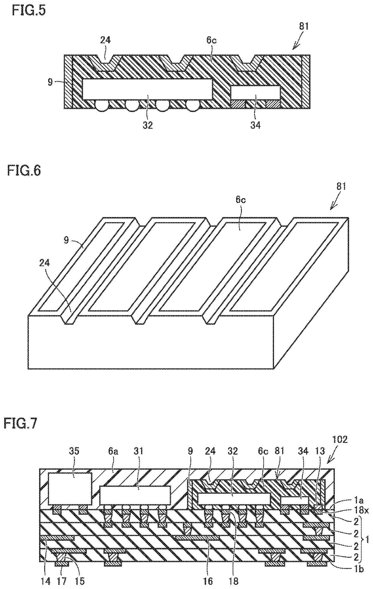
[0039]With reference to FIGS. 1 to 6, a module according to a first embodiment of the present disclosure will be described.
[0040]FIG. 1 illustrates the appearance of a module 101 according to the present embodiment. An upper surface and side surfaces of module 101 are covered with an external shielding film 8. FIG. 2 illustrates module 101 as viewed obliquely from below in FIG. 1. A lower surface of module 101 is not covered with external shielding film 8, and a substrate 1 is exposed from the lower surface. At least one external terminal 17 is provided on the lower surface of substrate 1. The number, size, and arrangement of external terminals 17 illustrated in FIG. 2 are merely examples. FIG. 3 illustrates a perspective plan view of module 101. FIG. 3 corresponds to a top view of module 101 with the upper surface on external shielding film 8 of module 101 removed, a first sealing resin 6a removed, and the upper surface on internal shielding film 9 of a sub-module 81 removed. A fir...
second embodiment
[0055]With reference to FIG. 8, a module according to a second embodiment of the present disclosure will be described. FIG. 8 is a cross-sectional view of a module 103 according to the present embodiment. Module 103 is identical in basic configuration to module 101, but differs in the following points.
[0056]Module 103 includes a sub-module 81i instead of sub-module 81. Sub-module 81i includes a sub-module substrate 11, second component 32 is mounted on a surface of sub-module substrate 11 remote from first surface 1a, and sub-module substrate 11 is mounted on first surface 1a. Sub-module substrate 11 includes a connection terminal 19 on a surface facing main substrate 1. Connection terminal 19 is electrically connected to pad electrode 18 provided on first surface 1a.
[0057]The present embodiment can produce the same effects as the effects of the first embodiment. In the present embodiment, since sub-module 81i includes sub-module substrate 11 as a unique substrate, unique wiring can...
third embodiment
[0058]With reference to FIG. 9, a module according to a third embodiment of the present disclosure will be described. FIG. 9 is a cross-sectional view of a module 104 according to the present embodiment. Module 104 is identical in basis configuration to module 101, but differs in the following points.
[0059]Module 104 includes a sub-module 81j instead of sub-module 81. None of the side surfaces of sub-module 81j is covered with internal shielding film 9.
[0060]The present embodiment can produce the same effects as the effects of the first embodiment. Such a configuration may be used when it is not strictly required to shield the sides of contained second component 32.
[0061]Internal shielding film 9 may be disposed so as to cover only some of the side surfaces of sub-module 81j, or alternatively, internal shielding film 9 need not be disposed at all on the side surfaces.
PUM
 Abstract
Description
Claims
Application Information


