Active matrix display with sealing material

a technology of sealing material and active matrix, applied in non-linear optics, instruments, optics, etc., can solve the problems of insufficient temperature resistance of the driver circuit and prone to contamination

Inactive Publication Date: 2000-01-04
SEMICON ENERGY LAB CO LTD
View PDF6 Cites 142 Cited by
  • Summary
  • Abstract
  • Description
  • Claims
  • Application Information

AI Technical Summary

Problems solved by technology

Therefore, the driver circuit does not have sufficient te

Method used


Image

  • Active matrix display with sealing material
  • Active matrix display with sealing material
  • Active matrix display with sealing material

Examples


example 2

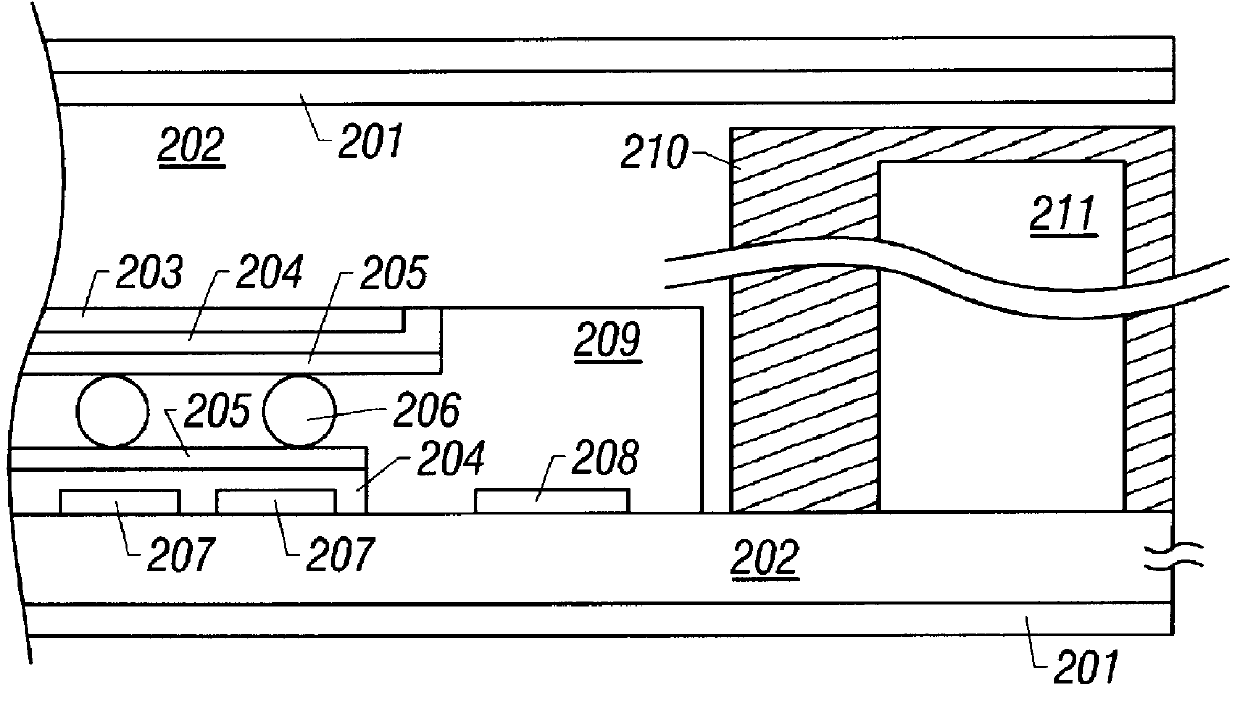
Another active matrix display according to the present invention is shown in FIG. 3 in cross section. As can be seen from this figure, a microprocessor 311 for controlling the active matrix display and TFTs 308 forming a driver circuit are sealed by a sealing material 310, thus protecting the driver circuit TFTs 308. The driver circuit TFTs 308 are prevented from being exposed. The present example is similar to Example 1 in structure and process sequence except for circuit elements (driver circuit TFTs 308) sealed by the sealing material 310.

example 3

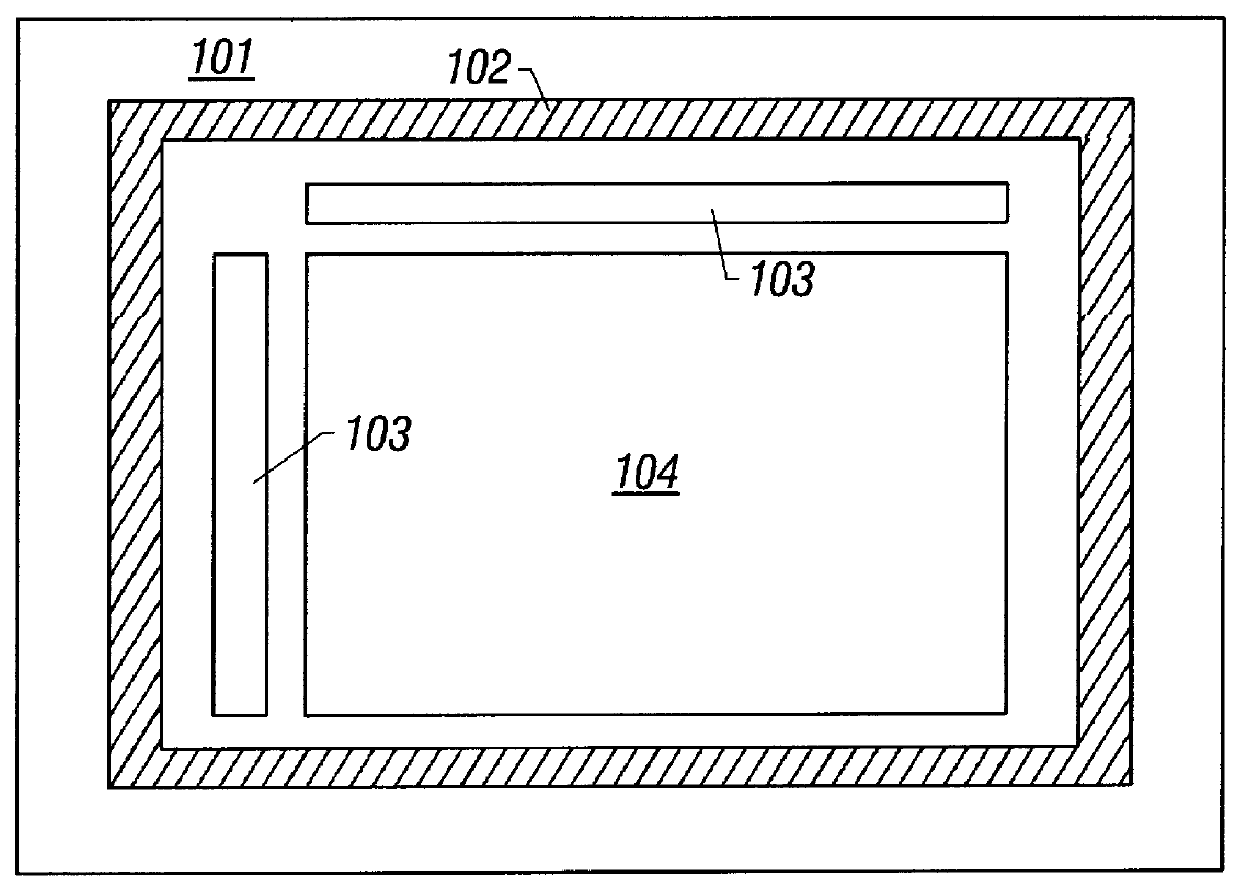
The present example pertains to a structure equipped with a preliminary peripheral circuit (redundant circuit). FIG. 7 is a schematic top view of a liquid crystal panel according to the present example. Since FIG. 7 is a view taken from the top, only one glass substrate 701 is shown. In practice, however, another glass substrate which makes a pair with the glass substrate 701 is bonded to the glass substrate 701. In the structure shown in FIG. 7, a peripheral driver circuit region 703 and a matrix pixel region 704 are located inside a sealing material 702. Since the inside of the sealing material 702 is filled with a liquid crystal material, the liquid crystal material exists on the top surfaces of the TFTs arranged in the peripheral driver circuit region 703 and in the pixel region 704.

An integrated circuit (IC) forming various control circuits connected with the peripheral driver circuit is positioned within the sealing material 702 and just molded in this sealing material 702.

Ind...

example 4

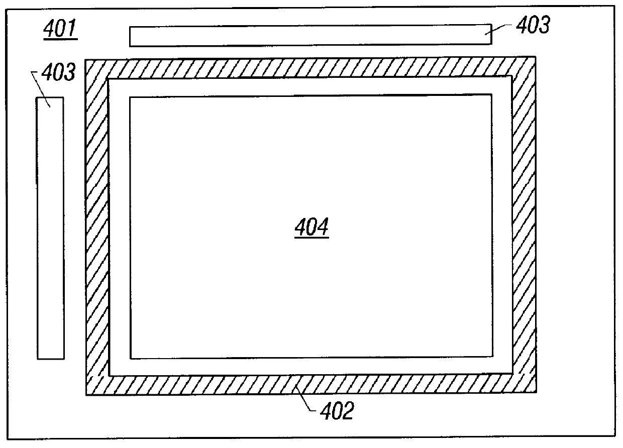
FIG. 8 shows an embodiment in which a single glass substrate 801 is constituted of four panels. The substrate shown in FIG. 8 is constituted of a peripheral drive circuit 803 and a pixel area 804 which are integrated on the same glass substrate. The pixel area 804 is constituted of at least one thin-film transistor which is connected to a pixel electrode arranged like a matrix.

In FIG. 8, only the glass substrate 801 on which each circuit is formed is shown, however, another glass substrate opposite to it is actually arranged. A counter electrode is arranged on the opposite glass substrate not shown.

Further, in the constitution shown in FIG. 8, the active matrix liquid display device is divided by sealing material 802 so as to realize a manufacturing of a plurality of active matrix liquid crystal display panels on a pair of glass substrates. With such a constitution, the productivity and the reliability can be simultaneously enhanced.

It should be noted that although the width of the ...


PUM


Abstract

An active matrix liquid crystal display having improved reliability. Pixel regions and a peripheral driver circuit are integrally packed on the display. TFTs forming the peripheral driver circuit are located inside a sealing material layer on the side of a liquid crystal material, thus protecting the peripheral driver circuit from external moisture and contaminants. This enhances the long-term reliability of the peripheral driver circuit. Pixel TFTs are arranged in pixel regions. The leads going from the TFTs forming the peripheral driver circuit to the pixel TFTs are shortened. This results in a reduction in the resistance. As a result, the display characteristics are improved.

Description

1. Field of the InventionThe present invention relates to techniques for miniaturizing active matrix displays and for enhancing their reliability.2. Description of the Related ArtThe state of a panel forming the prior art active matrix display is shown in FIG. 4 in cross section. As can be seen from this figure, a sealing material 402 surrounds a pixel region 404 and so only the pixel region 404 of the active matrix display is in contact with a liquid crystal material. TFTs in a peripheral driver circuit region 403 are in contact with the atmosphere. These are remains of the prior art techniques in which only pixel TFTs are present on the substrate of an active matrix display, and in which a driver circuit is an externally attached IC. In these prior art techniques, the position at which the driver circuit is mounted is not optimized where the pixel region 404 and the peripheral driver circuit region 403 are formed on the same glass substrate 401.In the prior art active matrix displ...

Claims


Application Information

Patent Timeline
IPC IPC(8): G02F1/1362G02F1/13G02F1/1339
CPCG02F1/13454G02F1/1339
Inventor YAMAZAKI, SHUNPEIKOYAMA, JUNKAWASAKI, YUJIKONUMA, TOSHIMITSUTERAMOTO, SATOSHIHIRAKATA, YOSHIHARU
Owner SEMICON ENERGY LAB CO LTD
Why Eureka
Try Eureka