Active-matrix type liquid-crystal display
- Summary
- Abstract
- Description
- Claims
- Application Information
AI Technical Summary
Problems solved by technology
Method used
Image
Examples
first embodiment
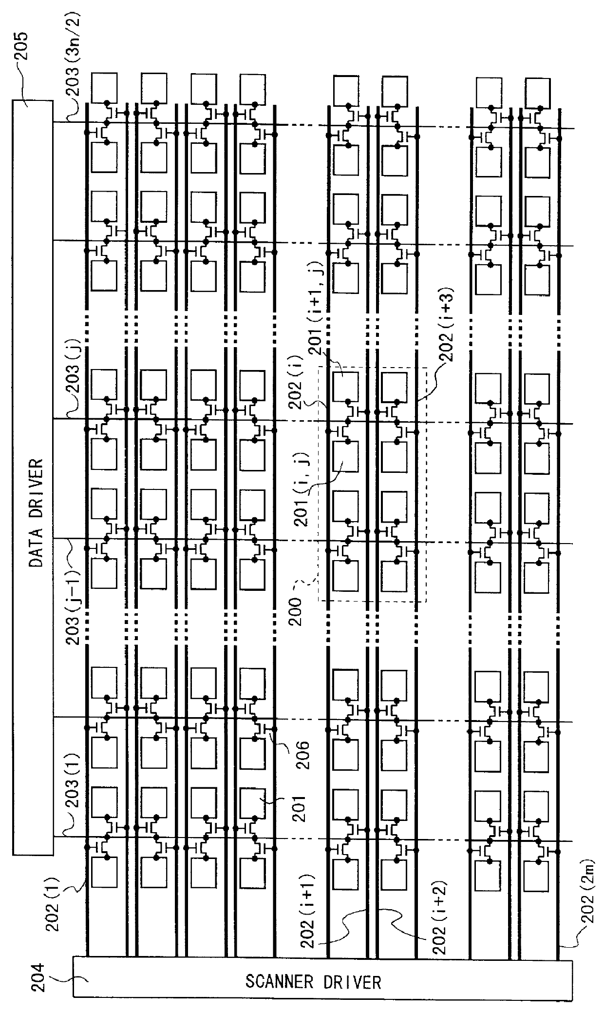
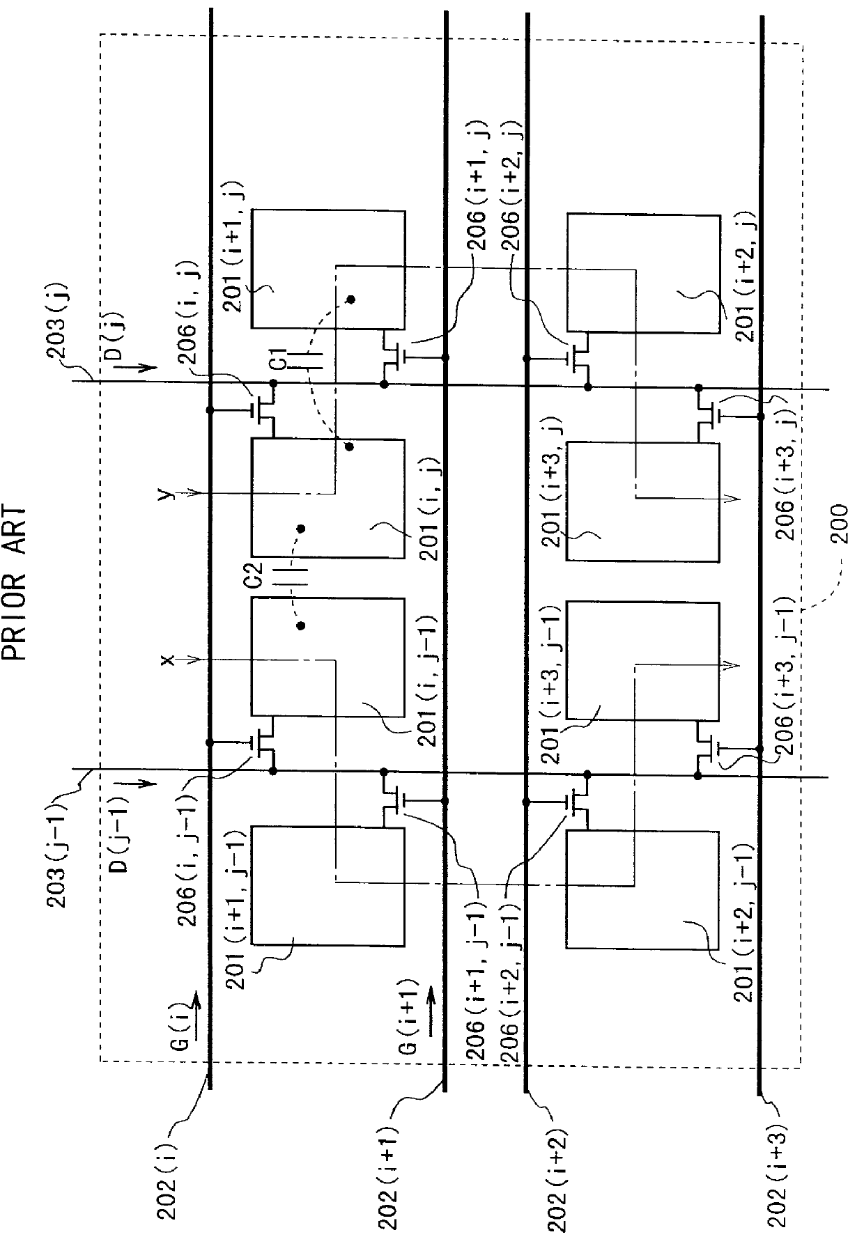
A color LCD has a configuration as shown in FIG. 10A.
As shown in FIG. 10A, a plurality of pixel electrodes 1 are arranged in a matrix array with 2m rows and (3 / 2)n columns. The total number of these pixel electrodes 1 is 3(m.times.n).
A group of the [(2 / 3)m.times.(1 / 2)n] pixel electrodes 1 are used for displaying the red (R) color, forming R subpixels. Another group of the [(2 / 3)m.times.(l / 2)n] pixel electrodes 1 are used for displaying the green (G) color, forming G subpixels. The remaining [(2 / 3)m.times.(1 / 2)n] pixel electrodes 1 are used for displaying the blue (B) color, forming B subpixels. Thus, the total number of pixels or dots of this color LCD is (m.times.n) (=3[(2 / 3)m.times.(1 / 2)n]).
First to 2m-th scanning lines 2(1) to 2(2m) are arranged along the respective rows of the matrix array. First to (3 / 2)n-th data lines 3(1) to 3(3n / 2) are arranged along the respective columns of the matrix array. 3(m.times.n) TFTs 6 are arranged at the respective intersections of the scanning ...
second embodiment
FIGS. 13, 14, and 15 show a color LCD according to a second embodiment. This LCD has the same configuration as that of the first embodiment other than the pattern and structure of the fixed-potential electrodes. Therefore, the explanation about the same configuration is omitted here by attaching the same reference numerals or characters to the same and corresponding elements in FIGS. 13, 14, and 15 for the sake of simplification of description.
As shown in FIGS. 13, 14, and 15, an electrically conductive film 7' is formed on the gate insulating film 15, not on the glass substrate 16. The pixel electrodes 1 are formed on the protection film 10. A passivation film 18 is formed on the film 10 to cover all the pixel electrodes 1.
The pixel electrodes 1 are electrically connected to the source electrodes 12 of the corresponding TFTs 6 through corresponding contact holes 8 formed In the passivation film 10.
The conductive film 7' has a pattern as clearly shown in FIG. 13. This conductive fil...
third embodiment
FIGS. 16, 17, and 18 show a color LCD according to a third embodiment. This LCD has a configuration obtained by adding another fixed-potential electrodes 11 to the LCD according to the first embodiment. Therefore, the explanation about the same configuration is omitted here by attaching the same reference numerals or characters to the same and corresponding elements in FIGS. 16, 17. and 18 for the sake of simplification of description.
As shown in FIGS. 16, 17, and 18, the fixed-potential electrodes 11 is formed on the gate insulating film 15, not on the glass substrate 16. The pixel electrodes 1 are formed on the same gate insulating film 15.
Each of the fixed-potential electrodes 11. which has a linear plan shape extending along the data lines 3(1) to 3(3n / 2), is located at the center of the corresponding fixed-potential electrode 7b. Each of the fixed-potential electrodes 11 is electrically connected to the underlying, corresponding fixed-potential electrode 7b through a contact ho...
PUM
 Abstract
Description
Claims
Application Information


