High performance cost optimized memory with delayed memory writes

a memory write and memory optimization technology, applied in the field of electronic systems for data storage and retrieval, can solve the problems of cost and performance compromise, lack of control resources, and relatively limited sequence of memory operations

Inactive Publication Date: 2000-06-13
RAMBUS INC +1
View PDF6 Cites 183 Cited by
  • Summary
  • Abstract
  • Description
  • Claims
  • Application Information

AI Technical Summary

Problems solved by technology

In any engineered design there are compromises between cost and performance.
The sequence of memory operations is relatively limited.
There may be other reasons to stall the memory requester, for example references to different rows of the same bank may introduce bank contention, but lack of control resources will not be a reason for stalling the memory requester
First, main memory traffic can be cached or uncached processor references. Such traffic is latency sensitive since typically a processor will stall when it gets a cache miss or for any other reason needs data fetched from main memory. Addressing granularity requirements are set by the transfer size of the processor cache which connects to main memory. A typical value for the cache transfer size is 32 bytes. Since multiple memory interfaces may run in parallel it is desirable that the memory system perform well for transfer sizes smaller than this. Main memory traffic is generally not masked; that is, the vast bulk of its references are cache replacements which need not be written at any finer granularity than the cache transfer size.
Latency is still important since longer latency requires larger buffers in the controller and causes other second order problems.
If small quanta cannot be accessed then bandwidth will be wasted transferring information which is not actually used.
There are many negative aspects to the increase in the length of the package wiring 1640, including the facts that: the overall size of the package must increase, which costs more to produce and requires more area and volume when the package is installed in the next level of the packaging hierarchy, such as on a printed circuit board.
Also, the stub created by the longer package wiring can affect the speed of the interconnect.
In addition, mismatch in package wiring lengths due to the fan-in angle can affect the speed of the interconnect due to mismatched parasitics.
For example, the memory device package requires more material, the next level of interconnect, such as a printed circuit board, requires more area, if connectors are used they will be more expensive, and the package and die area of the master device will grow.
In addition to all these cost concerns based on area and volume of the physical construction another cost concern is power.
Added power translates to added cost since the power must be both supplied and then dissipated with heat sinks.
When this register is set to its minimum value and the reference is anything besides a hit then the device has insufficient control bandwidth to specify all the required operations while simultaneously keeping the data pins highly utilized.
The technique of specifying the burst size in a register makes it difficult to mix transfer sizes unless the burst size is always programmed to be the minimum, which then increases control overhead.
The increase in control overhead may be so substantial as to render the minimum burst size impractical in many system designs.
A controller which has references in progress that are simultaneously ready to use the control resources must sequentialize them, leading to otherwise unnecessary delay.
As can be seen, the data pins are poorly utilized.
This indicates that control contention will limit the ability of the device to transfer data for various mixes of application references.
However, the applications, such as graphics applications, require small length transfers rather than large ones.
When writes and reads are mixed, this leads to difficulties in fully utilizing the data pins.
Thus, current memory devices have inadequate control bandwidth for many application reference sequences.
Current memory devices are unable to handle minimum size transfers.
Further, current memory devices utilize the available control bandwidth in ways that do not support efficient applications.
Current memory devices do not schedule the use of the data pins in an efficient manner.
In addition, current memory devices inefficiently assign a bonding pad for every pin of the device.

Method used


Image

  • High performance cost optimized memory with delayed memory writes
  • High performance cost optimized memory with delayed memory writes
  • High performance cost optimized memory with delayed memory writes

Examples


Embodiment Construction

FIG. 13 shows a timing diagram according to an embodiment of the present invention in which the Mask pins 2030 carry a precharge specification rather than either the write mask information or the tristate control information, as shown in connection with FIG. 12. This use of the Mask pins need not be exclusive. There are multiple ways in which to indicate how the information presented on the Mask pins is to be used. For example:

in one embodiment according to the present invention, a register within the device specifies whether the mask pins are to be used for masking, tristate control, or precharge control;

in another embodiment according to the present invention, the encoding of the command pins is extended to specify, on a per operation basis, how the mask pins are to be used; and

in another embodiment according to the present invention, a register bit indicates whether tristate control is enabled or not and, in the case it is not enabled, an encoding of the command pins indicates if...


PUM


Abstract

A memory device includes an interconnect with control pins and bidirectional data pins. A memory core stores data. A memory interface circuit is connected to the interconnect and the memory core. The memory interface circuit includes a delay circuit to establish a write delay during a memory core write transaction such that the memory core write transaction has a processing time that is substantially equivalent to a memory core read transaction. The delay circuit delays the memory core write transaction for a time corresponding to the time required for signals to travel on the interconnect.

Description

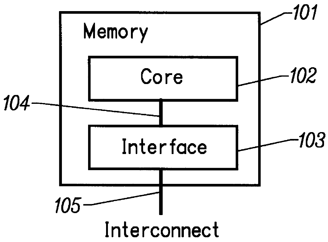
1. Field of the InventionThe present invention relates generally to electronic systems for data storage and retrieval. More particularly, the invention is directed toward improved methods and structures for memory devices.2. Description of the Related ArtIn any engineered design there are compromises between cost and performance. The present invention introduces novel methods and structures for reducing the cost of memory devices while minimally compromising their performance. The description of the invention requires a significant amount of background including: application requirements, memory device physical construction, and memory device logical operation.Memory device application requirements can be most easily understood with respect to memory device operation. FIG. 1 shows the general organization of a memory device. Memory device 101 consists of a core 102 and an interface 103. The core is responsible for storage of the information. The interface is responsible for translat...

Claims


Application Information

Patent Timeline
Patent Type & Authority Patents(United States)
IPC IPC(8): G11C7/10G11C7/00G11C7/22
CPCG11C7/1072G11C7/22G11C2207/229
Inventor BARTH, RICHARD M.WARE, FREDERICK A.STARK, DONALD C.HAMPEL, CRAIG E.DAVIS, PAUL G.ABHYANKAR, ABHIJIT M.GASBARRO, JAMES A.NGUYEN, DAVIDHOLMAN, THOMAS J.ANDERSON, ANDREW V.MACWILLIAMS, PETER D.
Owner RAMBUS INC
Why Eureka
Try Eureka