Nonvolatile semiconductor memory device and a method of fabricating the same

Inactive Publication Date: 2000-10-24
SANYO ELECTRIC CO LTD
View PDF4 Cites 16 Cited by
  • Summary
  • Abstract
  • Description
  • Claims
  • Application Information

AI Technical Summary

Problems solved by technology

However, such a nonvolatile semiconductor memory device has the following problem.
The memory device has a further problem in that a high accuracy is required in alignment of the floating gate 4 and the isolation film 2.
As a result, there arises a problem in that it is judged that the memory cell is in the erased state.
When, in order to cope with the problem, the size of the floating gate is increased, there arises a problem in that adjacent floating gates are contacted with each other because the gap between adjacent floating gates is very narrow as shown in FIG. 10.

Method used


Image

  • Nonvolatile semiconductor memory device and a method of fabricating the same
  • Nonvolatile semiconductor memory device and a method of fabricating the same
  • Nonvolatile semiconductor memory device and a method of fabricating the same

Examples


Embodiment Construction

Hereinafter, a nonvolatile semiconductor memory device of a first embodiment of the invention will be described with reference to the accompanying drawings. The components which are identical with those of the prior art are denoted by the same reference numerals and their description is omitted.

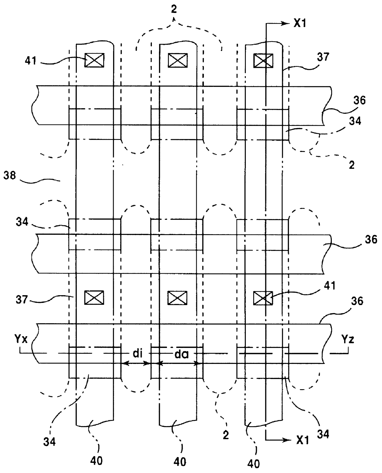
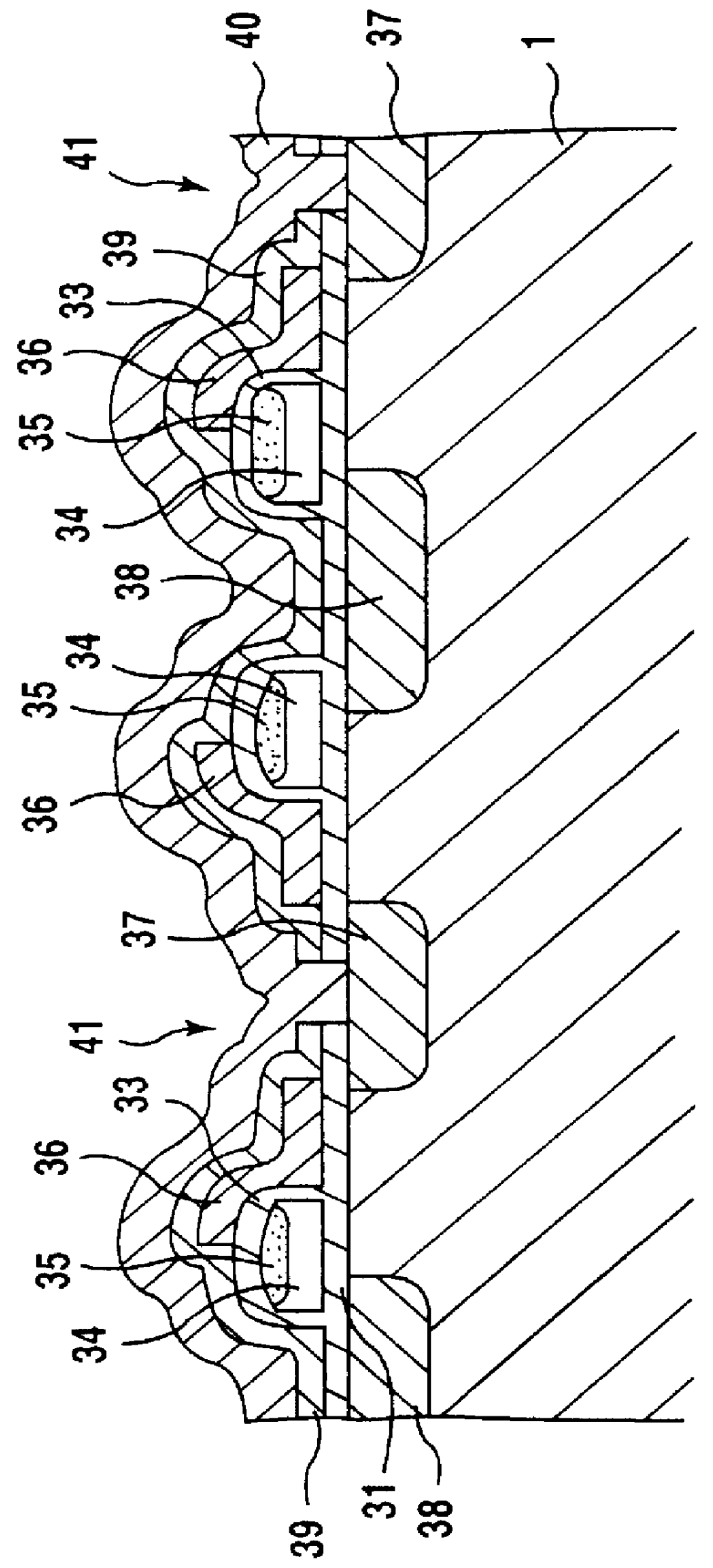
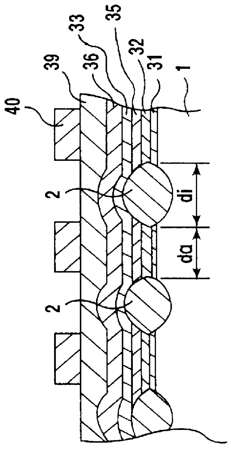
FIG. 1 is a top view of a memory cell of a nonvolatile semiconductor memory device having a floating gate, FIG. 2A is a cross sectional view taken along the line X1--X1 of FIG. 1, and FIG. 2B is a section view taken along the line Y1--Y1 of FIG. 1. These figures show a split gate structure in which a control gate is juxtaposed with a floating gate.

In a surface region of a P-type silicon substrate 1, plural isolation films 2 consisting of a LOCOS oxide film which is formed with being selectively thickened (from 4,000 to 8,000 angstroms) by the LOCOS (Local Oxidation Of Silicon) process are formed in a strip-like manner so as to partition the surface region into device regions. The isolation fi...


PUM


Abstract

A method of forming a nonvolatile semiconductor memory device of the present invention comprises: an isolation film formed on a semiconductor substrate of one conductivity type; a floating gate which is formed in an active region isolated by said isolation film so as to be disposed in a gap between adjacent isolation films and make each of end portions coincident with each end of said isolation film in a self-aligned manner; a tunnel oxide film which covers said floating gate; a control gate formed on said tunnel oxide film so as to comprise a region which overlaps said floating gate; a diffusion region of an opposite conductivity type and formed in a surface of the semiconductor substrate adjacent to said floating gate and the control gate.

Description

1. Field of the InventionThe present invention relates to a nonvolatile semiconductor memory device comprising an isolation film formed on a silicon substrate, a floating gate which is formed in an active region isolated by the isolation film and disposed in a gap between adjacent isolation film(s), and a control gate having a region which overlaps one end portion of the floating gate via a tunnel oxide film covering the floating gate, and also to a method of fabricating such a device.2. Description of the Related ArtIn a nonvolatile semiconductor memory device in which each memory cell consists of a single transistor and can be electrically erased, particularly in a programmable ROM (EEPROM: Electrically Erasable and Programmable ROM), each memory cell is formed by a transistor of a double gate structure having a floating gate and a control gate. In such a transistor of a double gate structure, a data is written by injecting hot electrons generated in the channel under the gap regi...

Claims


Application Information

Patent Timeline
IPC IPC(8): H01L21/28H01L27/115H01L21/70H01L21/02H01L29/40H01L29/423H01L21/8247H01L29/788H01L29/792
CPCH01L21/28273H01L29/42324H01L27/11521H01L27/115H01L29/40114H10B69/00H10B41/30
Inventor OYA, YUKIHIRO
Owner SANYO ELECTRIC CO LTD
Why Eureka
Try Eureka