

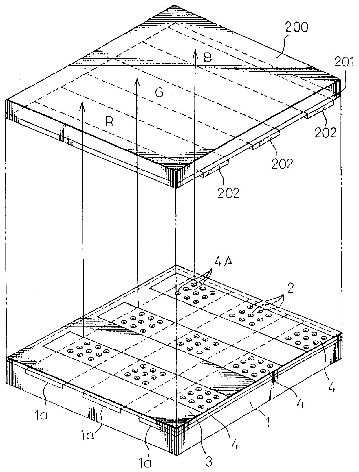
Cathode device having smaller opening
a cathode and opening technology, applied in the manufacture of electric discharge tubes/lamps, tubes with screens, discharge tubes luminescnet screens, etc., can solve the problem of difficult to make a mask 51 having a smaller diameter
- Summary
- Abstract
- Description
- Claims
- Application Information
AI Technical Summary
Problems solved by technology
Method used
Image

Examples
first embodiment
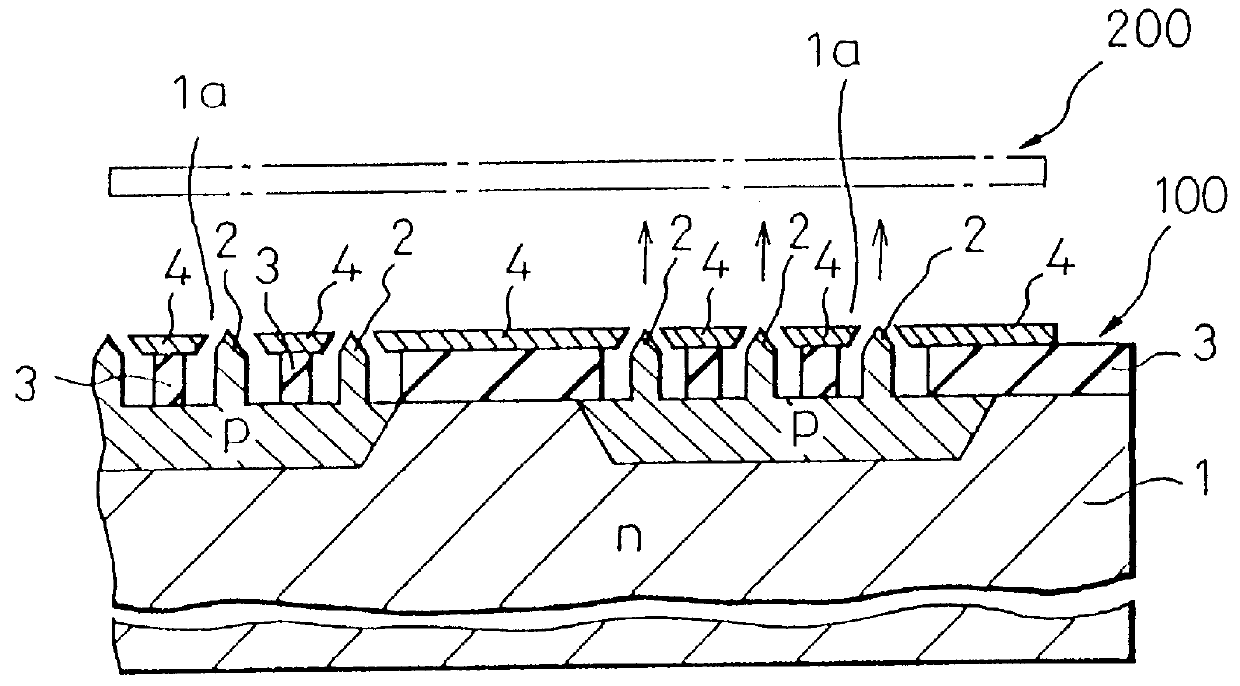
FIGS. 4 to 10 show consecutive steps in the method for fabricating the cathode device 100 of FIG. 1.
In FIG. 4, a silicon substrate 1 is prepared. The silicon substrate 1 is of an n-type, and a p-type region (or regions) 1a is formed on the surface of the silicon substrate 1, as described with reference to FIG. 2. Alternatively, a cathode electrode made of another conductor may be formed on the silicon substrate 1 via an insulating layer.
A layer of the mask for forming the emitter tip 2 is formed on the silicon substrate 1, for example, by a chemical vapor deposition (CVD) technique. In the embodiment, the mask layer comprises a two-layer structure comprising, for example, a first insulating layer 61 having a thickness of 300 nm and made of Si.sub.3 N.sub.4 and a second insulating layer 51 having a thickness of 300 nm and made of SiO.sub.2. The first insulating layer 61 is on the substrate 1, and the second insulating layer 51 is on the first insulating layer 61. A nitride such as Si...
fourth embodiment
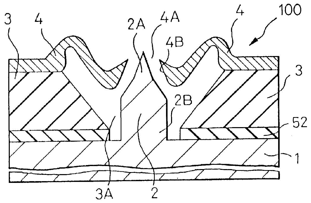
FIGS. 19A to 19C show the method for fabricating the cathode device 100. This embodiment is substantially identical to the embodiment shown in FIGS. 18A to 18E. FIG. 19A shows a condition after the mask 61 and 51 for the emitter tip 2 is formed on the silicon substrate 1 and given a desired mask pattern; the substrate 1 is etched using the mask 61 and 51 to form the emitter tip 2; and the insulating layer 3 is formed. Here, the emitter tip 2 comprises the conical tip end portion 2A and the cylindrical stem portion 2B. The oxide layer 52 has not yet been formed in this stage. Since the oxide layer 52 has not yet been formed, the emitter tip 2 does not swell (the emitter tip 2 may swell due to diffusion during the oxide layer forming step) and the shoulder of the emitter tip does not protrude beyond the contour of the mask 61 and 51. Therefore, the growing collar 10 is not parasitically produced in the insulating layer forming step.
In FIG. 19B, the substrate 1 is then immersed in a th...
fifth embodiment
FIGS. 20A to 20E show the method for fabricating the cathode device 100. FIG. 20A shows a condition after the mask 61 and 51 for the emitter tip 2 is formed on the silicon substrate 1 and given a desired mask pattern; the substrate 1 is etched using the mask 61 and 51 to form the emitter tip 2; and the oxide layer 52 is formed on the surfaces of the silicon substrate 1 and the emitter tip 2 to sharpen the emitter tip 2. In this embodiment, the emitter tip 2 is relatively short and substantially consists of the conical tip end portion 2A alone.
In FIG. 20B, the insulating layer 3 is formed after the oxide layer 52 has been formed. In this embodiment, since the shoulder of the emitter tip does not exist, the growing collar 10 is not parasitically produced in the insulating layer forming step.
In FIG. 20C, the substrate 1 is immersed in a thermal phosphoric acid etchant. The mask 61 and 51 is thus removed, while the insulating layer 3 is not dissolved but left unremoved.
In FIG. 20D, the ...
PUM
 Abstract
Description
Claims
Application Information