Apparatus and method for combining optical waveguide and optical fiber

a technology of applied in the field of apparatus and a method for combining optical waveguides and optical fibers, can solve the problem of taking a long time to align optical fibers and optical waveguides

Inactive Publication Date: 2000-12-12
SAMSUNG ELECTRONICS CO LTD
View PDF5 Cites 80 Cited by
  • Summary
  • Abstract
  • Description
  • Claims
  • Application Information

AI Technical Summary

Problems solved by technology

It is difficult and takes a long time to align the optical fibers and the optical waveguide, since the alignment must be performed with respect to an alignment axis having six degrees of freedom (it must be rotated with respect to three straight axes perpendicular to each other and three straight axes) with submicron precision.

Method used


Image

  • Apparatus and method for combining optical waveguide and optical fiber
  • Apparatus and method for combining optical waveguide and optical fiber
  • Apparatus and method for combining optical waveguide and optical fiber

Examples


Embodiment Construction

)

Hereinafter, a preferred embodiment of the present invention will be described in detail with reference to the attached drawings.

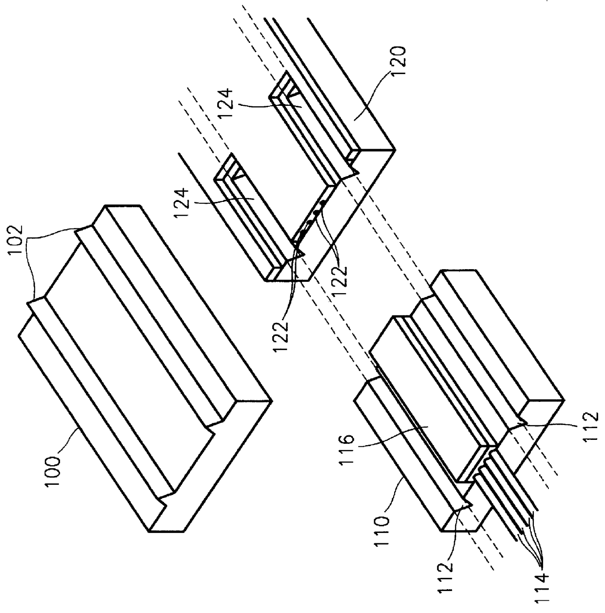
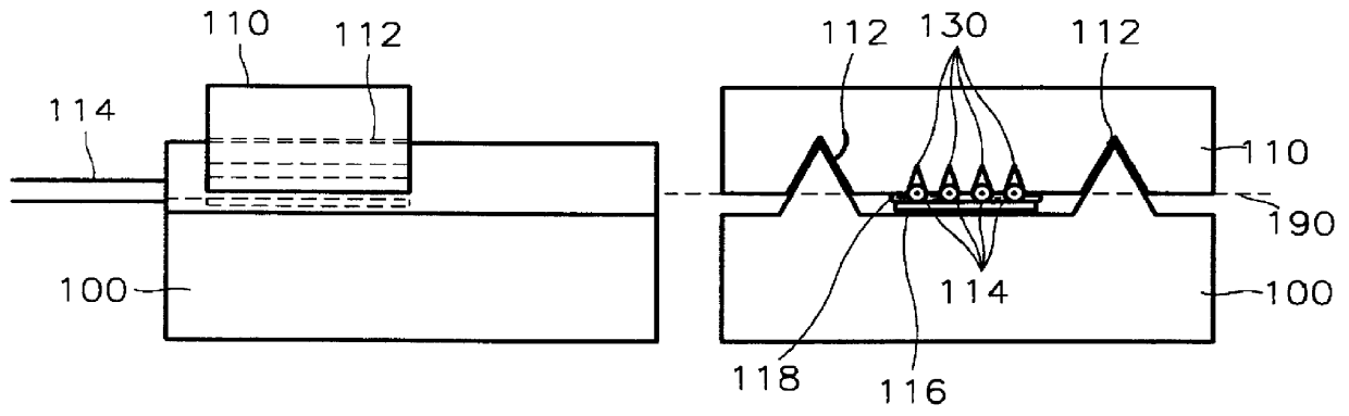
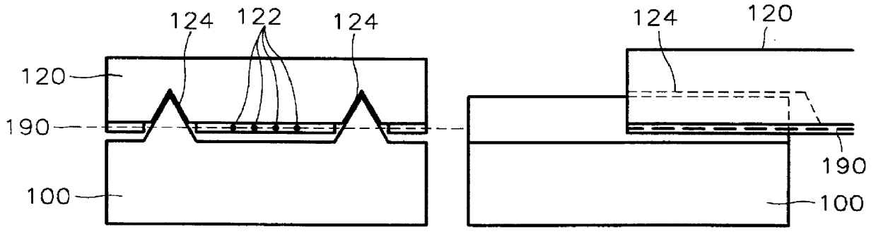
FIG. 1 is a block diagram showing the structure of an embodiment of an apparatus for combining optical fibers with an optical waveguide according to the present invention. The apparatus includes a guide rail portion 100, an optical fiber array portion 110 having a guide groove for alignment 112, and an optical waveguide device chip 120 having a guide groove for alignment 124.

The guide rail portion 100 includes guide rails 102 for alignment, spaced apart from each other by a predetermined distance, on a flat substrate. As shown in FIG. 1, two rails manufactured to be convex on a silicon substrate are spaced from each other by a predetermined distance.

In a preferred embodiment of manufacturing the guide rail 102, a strip pattern is formed of SiO.sub.2 or Si.sub.3 N.sub.4 to have an appropriate width, in a portion of a silicon substrate in which a convex rai...


PUM


Abstract

An apparatus and a method for combining an optical waveguide and optical fibers are provided. The apparatus includes an apparatus for combining optical fibers with an optical waveguide device, including a guide rail portion for alignment including guide rails for alignment spaced apart from each other by a predetermined distance, on a flat substrate, an optical fiber array portion put on the guide rail portion for alignment when the optical fibers are combined with the optical waveguide device, including an array of grooves for arranging the optical fibers spaced apart from each other by a predetermined distance in an array pattern, and including guide grooves for alignment having a concavo-convex relationship with the guide rail portion for alignment, and an optical waveguide device chip put on the guide rail portion when the optical fibers are combined with the optical waveguide, including the optical waveguide connected to the optical fibers of the optical fiber array portion, and including guide grooves for alignment spaced apart from each other by the same distance as that by which the rails of the guide rail portion are spaced apart from each other and having a concavo-convex relationship with the guide rail portion for alignment, to the outside of an optical waveguide area in which the cores of the optical fibers of the optical fiber array portion respectively coincide with those of the optical waveguide. According to the present invention, a light source and a photodetector (required for active alignment) are not necessary. A complicated alignment process of performing an alignment with respect to an alignment axis having six degrees of freedom with submicron precision is not necessary. Also, it is possible to save time and money when attaching the optical fibers to the optical waveguide device chip.

Description

1. Field of the InventionThe present invention relates to an apparatus and a method for combining an optical waveguide and optical fibers, and more particularly, to an apparatus for combining manually aligned optical fibers with an input and output optical waveguide of an integrated optical device manufactured by integrating an optical waveguide device having various functions with a substrate and a method therefor.2. Description of the Related ArtIn general, there are two methods for attaching optical fibers to an optical waveguide device. In a method referred to as an active alignment method, input light is guided to optical fibers or an element, the position of the optical fibers is precisely controlled, optical power in an optical waveguide or in an output waveguide of the optical fibers is measured, and the optical fibers and the optical waveguide are fixed in a state in which the combination of the optical fibers with the optical waveguide maximizes light transmission. In a pa...

Claims


Application Information

Patent Timeline
Patent Type & Authority Patents(United States)
IPC IPC(8): G02B6/30G02B6/36
CPCG02B6/30
Inventor YOU, BYONG-GWONLEE, HYUNG-JAERHEE, TAE-HYUNGLEE, YONG-WOO
Owner SAMSUNG ELECTRONICS CO LTD
Why Eureka
Try Eureka