High-performance IEEE1149.1-compliant boundary scan cell

a boundary scan and integrated circuit technology, applied in the field of integrated circuits, can solve the problems of circuit card testing expense, circuit card testing fixture complexity, and significant expense incurred

Inactive Publication Date: 2001-02-06
IBM CORP
View PDF12 Cites 32 Cited by
  • Summary
  • Abstract
  • Description
  • Claims
  • Application Information

AI Technical Summary

Problems solved by technology

A significant expense incurred during the manufacture of circuit cards carrying one or more integrated circuit components is testing.
Several factors contribute to the expense of circuit card testing.
First, because many circuit card components do not employ a standard I / O interface, circuit card testing fixtures tend to be complex and must often be custom-designed to test particular circuit cards.
Third, while it may be less expensive for a circuit card or component manufacturer to out-source testing to an outside contractor, the use of non-standard component interfaces can require the component manufacturer to reveal proprietary information concerning the internal design of a component to the component tester, making many manufacturers reluctant to engage an outside contractor to perform testing.
Because of the performance penalty associated with conventional IEEE1149.1-compliant boundary scan cells, manufacturers have resisted compliance with the IEEE1149.1 standard for at least eight years.

Method used


Image

  • High-performance IEEE1149.1-compliant boundary scan cell
  • High-performance IEEE1149.1-compliant boundary scan cell
  • High-performance IEEE1149.1-compliant boundary scan cell

Examples


Embodiment Construction

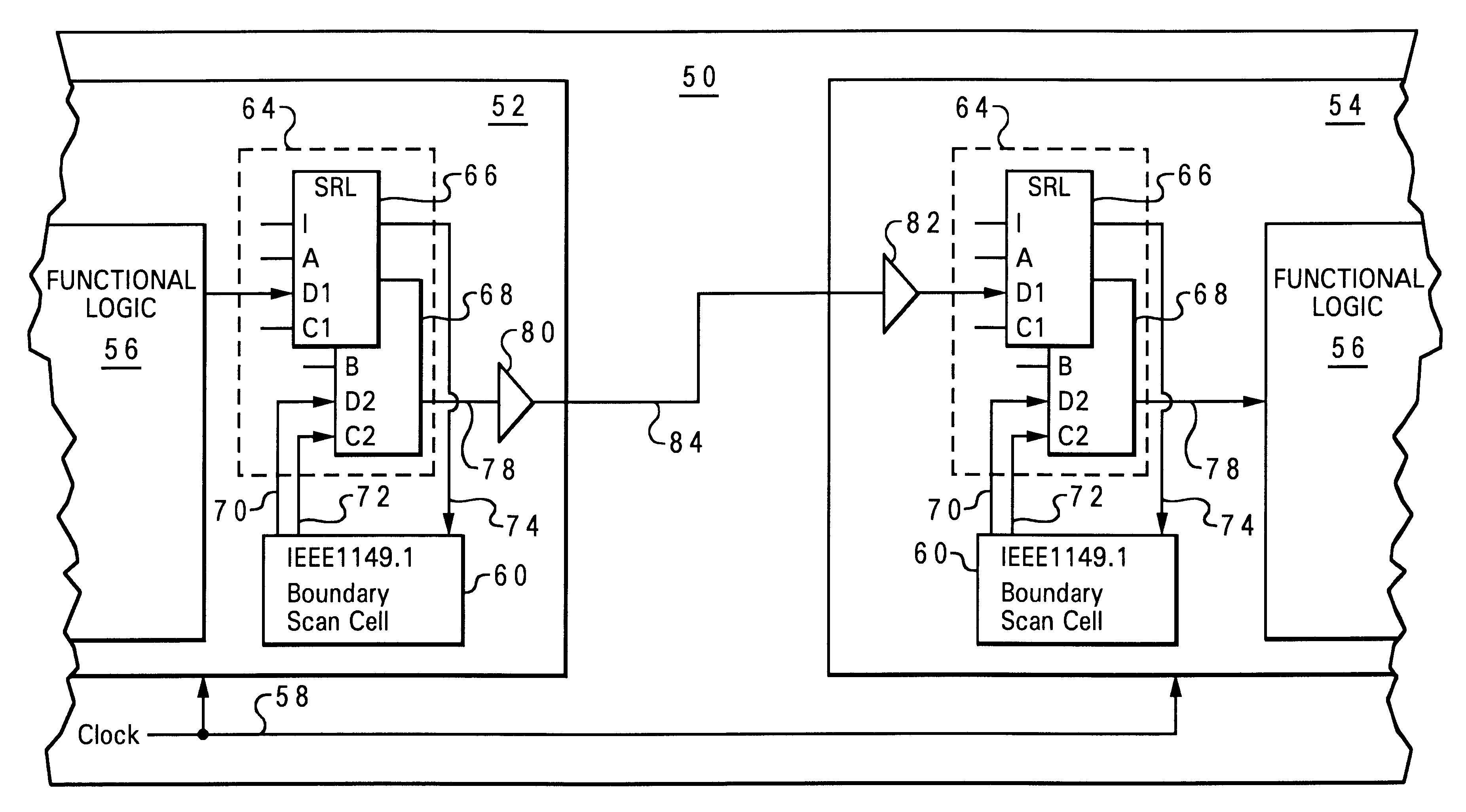
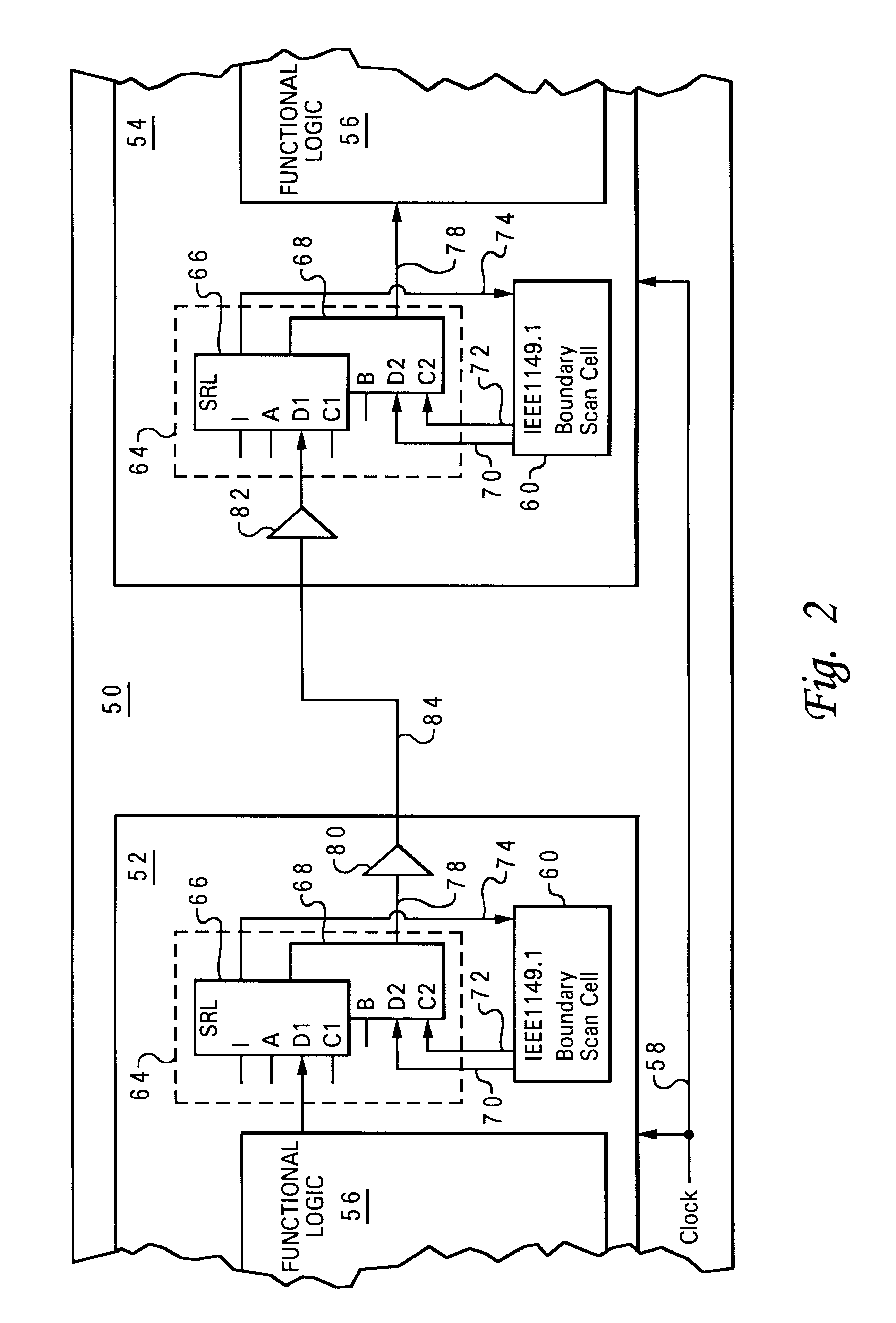
With reference again to the figures and in particular with reference to FIG. 2, there is depicted a high level block diagram of a circuit card on which are mounted interconnected integrated circuit chips that each include IEEE1149.1-compliant boundary scan cells in accordance with the present invention. Thus, as shown, a first integrated circuit chip 52 and a second integrated circuit chip 54 are each mounted on a circuit card 50. The function of each of integrated circuit chips 52 and 54 is determined by its respective functional logic 56. For example, integrated circuit 52 may comprise a processor and integrated circuit chip 54 may comprise a cache memory, ASIC (Application Specific Integrated Circuit), or other support chip. In the illustrated embodiment, the operation of integrated circuit chips 52 and 54 is synchronized by clock signal 58.

As shown in FIG. 2, integrated circuit chips 52 and 54 are each equipped with an IEEE1149.1-compliant boundary scan cell 60. However, in cont...


PUM


Abstract

A circuit is disclosed that includes a latch circuit and boundary scan cell circuitry. The latch circuit includes a slave latch and a master latch having a data output. The slave latch includes at least a first data input connected to the data output of the master latch, a second data input, and a control input that receives a control signal that controls latching of data present at the second data input. The boundary scan cell circuitry is connected to the second data input and to the control input of the slave latch so that the boundary scan cell circuitry can supply the control signal and data to the slave latch. In one embodiment, the boundary scan cell circuitry is IEEE1149.1-compliant and the circuit further includes either an output driver coupled to the data output of the slave latch or an input receiver coupled to a data input of the master latch.

Description

1. Technical FieldThe present invention relates in general to integrated circuitry and, in particular, to a boundary scan cell of an integrated circuit. Still more particularly, the present invention relates to a high-performance IEEE1149.1-compliant boundary scan cell of an integrated circuit.2. Description of the Related ArtA significant expense incurred during the manufacture of circuit cards carrying one or more integrated circuit components is testing. Such testing generally entails stimulating the input / output (I / O) pins of a circuit card with a predetermined pattern of inputs and then observing the outputs generated by the components residing on the circuit card. Several factors contribute to the expense of circuit card testing. First, because many circuit card components do not employ a standard I / O interface, circuit card testing fixtures tend to be complex and must often be custom-designed to test particular circuit cards. Second, the input pattern utilized to stimulate a ...

Claims


Application Information

Patent Timeline
Patent Type & Authority Patents(United States)
IPC IPC(8): G01R31/28G01R31/3185
CPCG01R31/318541
Inventor BARNHART, CARL FREDERICK
Owner IBM CORP
Why Eureka
Try Eureka