
Early voltage and beta compensation circuit for a current mirror

Inactive Publication Date: 2001-02-27
ANALOG DEVICES INC
View PDF10 Cites 18 Cited by
  • Summary
  • Abstract
  • Description
  • Claims
  • Application Information

AI Technical Summary

Benefits of technology

It is a further object of this invention to provide such a compensation circuit which cancels base current errors and base current modulation errors in a single circuit which is simple and easily implemented.
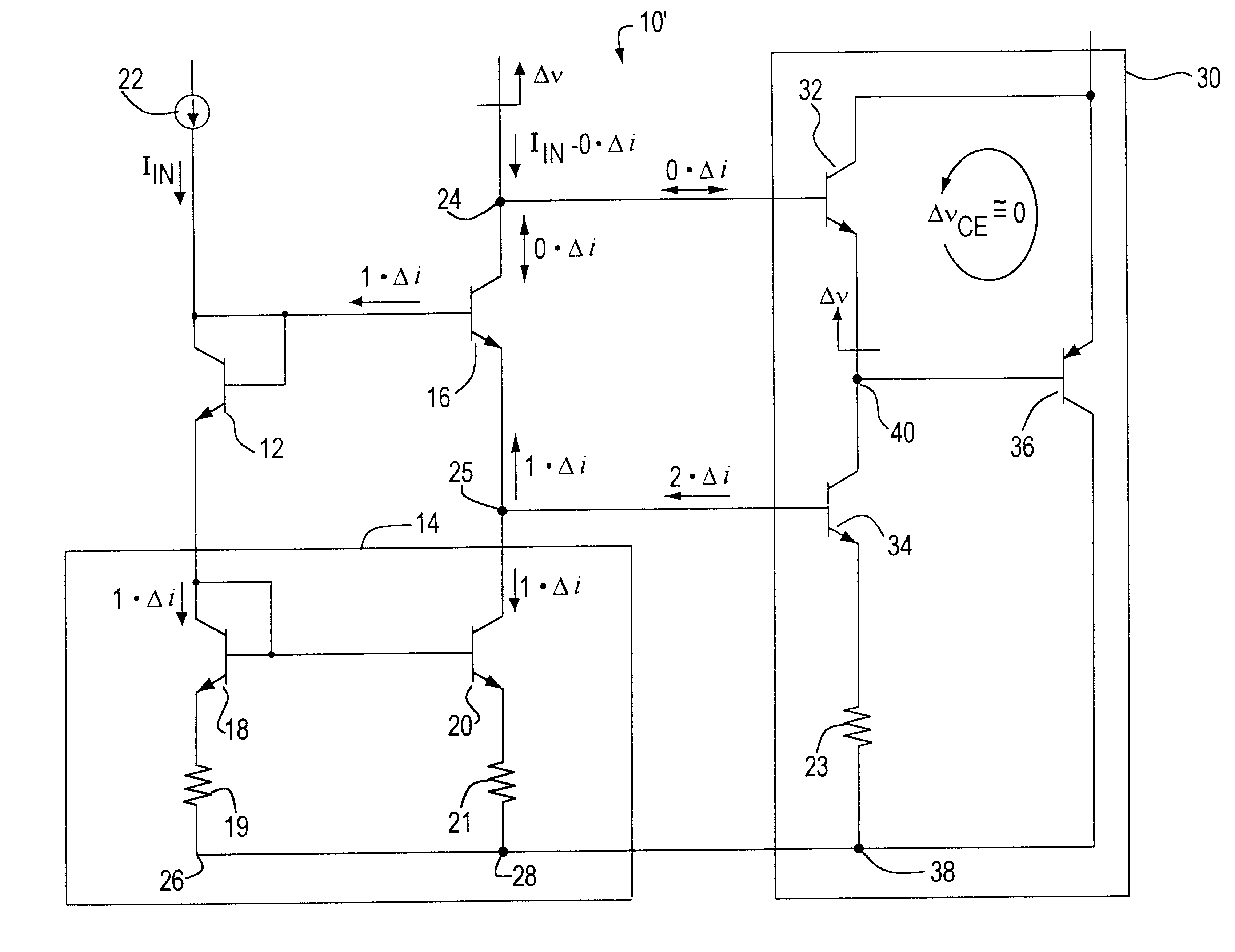
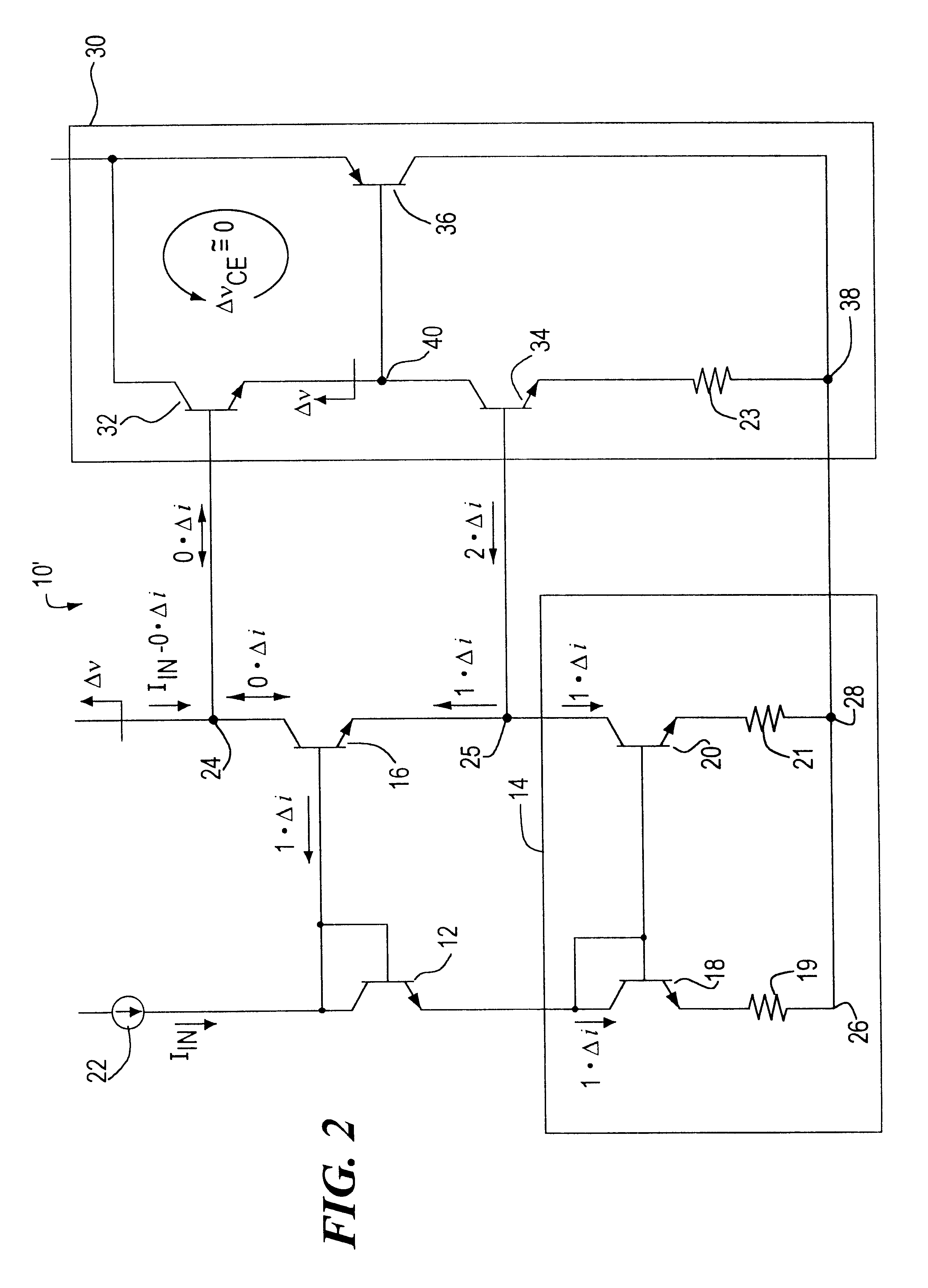
This invention features an Early voltage and beta compensated cascode current mirror. There is a cascode current mirror including an input stage, responsive to an input current, a current mirror circuit having a first stage responsive to the input stage and a second stage responsive to the first stage, and an output stage responsive to the second stage for providing an output voltage and current. There is a compensation circuit, responsive to the cascode current mirror, including a first compensation stage, a second compensation stage and a bootstrapping buffer stage, the first compensation stage, in response to a change in the output voltage, impresses a corresponding change in voltage on the second compensation stage, the second compensation stage thereby providing a change in current to the cascode current mirror for cancelling current errors induced by base current modulation in the output stage. The bootstrapping buffer, in response to the change in voltage, impresses an equal change in voltage on the first compensation stage to prevent errors from base current modulation effects in the first compensation stage. The first and second compensation stages further provide base current to the cascode current mirror for cancelling base current errors in the output current induced by the cascode current mirror.
The invention also features a beta current and Early voltage compensation circuit for a current mirror with an output stage for providing an output voltage and current gain Y. There is a first compensation stage, responsive to a change in the output voltage; a second compensation stage, responsive to the first compensation stage, for providing a current to the output stage; and a bootstrapping buffer, responsive to the change in output voltage, the first compensation stage, in response to the change in the output voltage, impresses an equal change in voltage on the second compensation stage, the second compensation stage thereby providing a change in current to the current mirror for cancelling current errors induced by base current modulation in the output stage. The bootstrapping buffer, in response to the change in voltage, impresses a corresponding change in voltage on the first compensation stage to prevent errors from base current modulation effects in the first compensation stage, the first and second compensation stages further providing a base current to the cascode current mirror for cancelling base current errors in the output current by the cascode current mirror.

Problems solved by technology

However, inherent problems prevent the output current from identically matching the input current.
Two problems in particular, base currents and base current modulation, contribute undesirable variations to the output current which result in an output current which does not follow the input current.
In contrast, finite Early voltage and changes in the mirror output voltage lead to base current modulation errors.
While it has been possible to compensate for each of these respective errors individually, to date, it has not been possible to easily cancel both errors with a single, simple compensation circuit.

Method used


Image

  • Early voltage and beta compensation circuit for a current mirror
  • Early voltage and beta compensation circuit for a current mirror
  • Early voltage and beta compensation circuit for a current mirror

Examples


Embodiment Construction

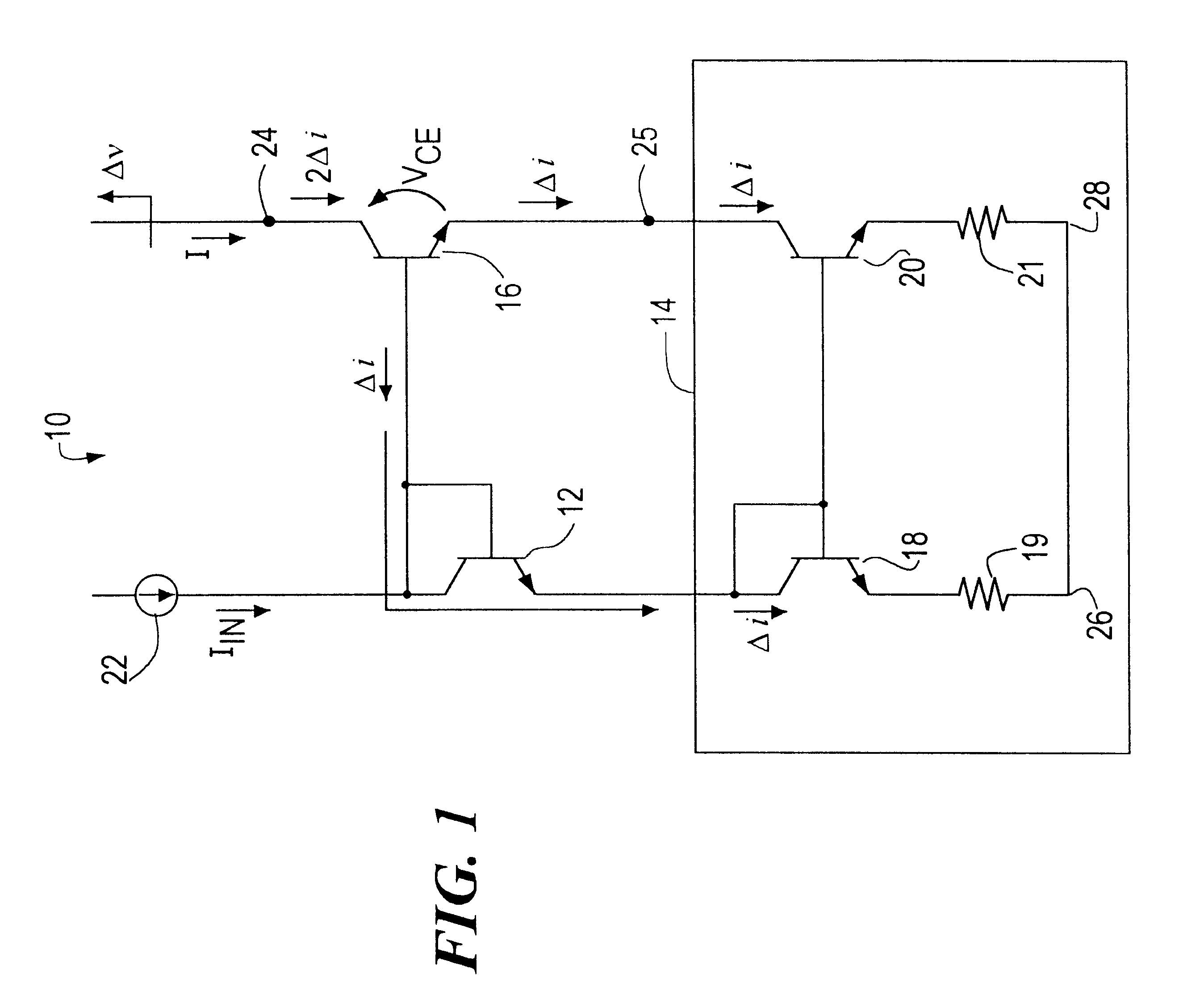
Prior art uncompensated cascode current mirror 10, FIG. 1, includes input transistor stage 12, simple current mirror 14 and output transistor stage 16. Current mirror 14 includes first transistor stage 18 and second transistor stage 20. Current mirror 14 may also include degeneration resistors 19 and 21, their presence improving the accuracy of current mirror 14. Current mirror 14 provides a current gain substantially equal to Y which is the ratio of the collector current of transistor 20 to the collector current of transistor 18. Transistors 12 and 18 form first leg 26, and transistors 16 and 20 form second leg 28 of cascode mirror 10. Legs 28 and 26 are defined to carry a normalized nominal current of Y to 1, respectively. While each transistor is shown to include an NPN semiconductor device, they may equally be PNP semiconductor devices. In any case, both types of devices, which include a control terminal, and first and second load terminals, e.g., base, collector and emitter, wi...


PUM


Abstract

An Early voltage and beta current compensated cascode current mirror includes a cascode current mirror having an input stage responsive to an input current, a current mirror circuit having a first stage responsive to the input stage and a second stage responsive to the first stage, and an output stage responsive to the second stage for providing an output voltage and current; and a compensation circuit, responsive to the cascode current mirror, having a first compensation stage, a second compensation stage and a bootstrapping buffer, the first compensation stage, in response to a change in the output voltage, impressing a corresponding change in voltage on the second compensation stage, the second compensation stage thereby providing a change in current to the cascode current mirror for cancelling current errors induced by base current modulation in the output stage, the bootstrapping buffer, in response to the change in voltage, impressing a corresponding change in voltage on the first compensation stage to prevent errors from base current modulation effects in the first compensation stage, the first and second compensation stages further providing a base current to the cascode current mirror for cancelling base current errors in the output current induced by the cascode current mirror.

Description

This invention relates to current mirrors and more particularly to a compensation circuit for a cascode current mirror for cancelling Early voltage and base current errors.BACKGROUND OF INVENTIONMany circuits rely on current mirrors for providing replicas of some input current. Current mirrors are designed to provide an output current which follows, or mirrors, the input current, or is a multiple thereof. However, inherent problems prevent the output current from identically matching the input current. Two problems in particular, base currents and base current modulation, contribute undesirable variations to the output current which result in an output current which does not follow the input current. Base currents, and hence base current errors, result from finite transistor beta. In contrast, finite Early voltage and changes in the mirror output voltage lead to base current modulation errors. While it has been possible to compensate for each of these respective errors individually,...

Claims


Application Information

Patent Timeline
IPC IPC(8): G05F3/08G05F3/26
CPCG05F3/265
Inventor D'AQUINO, STEFANO I.BROKAW, ADRIAN P.TAM, KIMO Y. F.WHITNEY, DAVID H.
Owner ANALOG DEVICES INC
Learn More