Dual damascene flowable oxide insulation structure and metallic barrier

a flowable oxide and damascene technology, applied in the field of flowable oxide (fox) layers, can solve the problems of rapid propagation cracks from relatively minor physical damage, unprotected fox materials are not generally considered suitable for formation of layers, and most fox materials are readily attacked

Inactive Publication Date: 2001-04-24
INT BUSINESS MASCH CORP
View PDF11 Cites 28 Cited by
  • Summary
  • Abstract
  • Description
  • Claims
  • Application Information

AI Technical Summary

Benefits of technology

It is also an object of the present invention to protect the surfaces of a FOX from processing steps and materials that degrade the FOX during the fabrication of semiconductor devices.
A similar object of the present invention is to provide a barrier improving the function of a secondary metallic barrier.
A further object of the present invention is to increase the adhesion between a FOX and a material deposited on the FOX during the fabrication of a semiconductor device.
Yet another related object of the present invention is to provide a very thin protective barrier formed by oxidizing an oxide.

Problems solved by technology

While the dielectric constant is low, the bridging oxygen atoms are strained and can be attacked by numerous chemicals or result in rapidly propagating cracks from relatively minor physical damage.
For that reason, unprotected FOX materials are not generally considered suitable for formation of layers even though they exhibit good planarizing characteristics that would support high resolution lithographic processes.
However, most FOX materials are readily attacked by most lithographic resist developers which are generally of high pH.
Moreover, when the FOX material is attacked by resist developers, the amount of material which may be removed is not readily controllable and may undercut the resist pattern.
Thus, when the FOX is etched, even with a well-controlled etchant, the resulting via shape may be quite distorted and vias will lack uniformity across the chip and possibly be irregularly and unreliably registered with the structures on the chip to which the vias are to form connections.
Moisture is similarly damaging to FOX materials.
Unfortunately, this exposure causes other reliability problems associated with the extrusion of the metallic conductor into the FOX or corrosion of the metallic conductor or both.
For example, when the conductive paths in an integrated circuit chip are at close pitch, even a very small amount of copper extrusion through a pinhole defect can cause a short circuit between one copper interconnect line and a second copper interconnect line.
Protection of the surface of the FOX material with a further layer of material such as another dielectric is not practical in some semiconductor structures such as formation of connection vias in a dual Damascene process.
However, the dielectric constant of the volume of FOX material converted to oxide is increased which increases the capacitance.
Similarly, the provision of a separate protective layer of another material would significantly alter the average dielectric constant and potentially introduce adhesion problems.
Thus, there is a need for a very thin protective barrier which cannot be formed by previously known methods.
No technique has been available for avoiding the basic incompatibility of FOX materials and resist developers in processes requiring a sequence of patterned etch steps, such as in a dual damascene process, particularly for accommodating fine pitch design rules for high density integrated circuits where the low dielectric constant of FOX materials is particularly critical.

Method used


Image

  • Dual damascene flowable oxide insulation structure and metallic barrier
  • Dual damascene flowable oxide insulation structure and metallic barrier
  • Dual damascene flowable oxide insulation structure and metallic barrier

Examples


Embodiment Construction

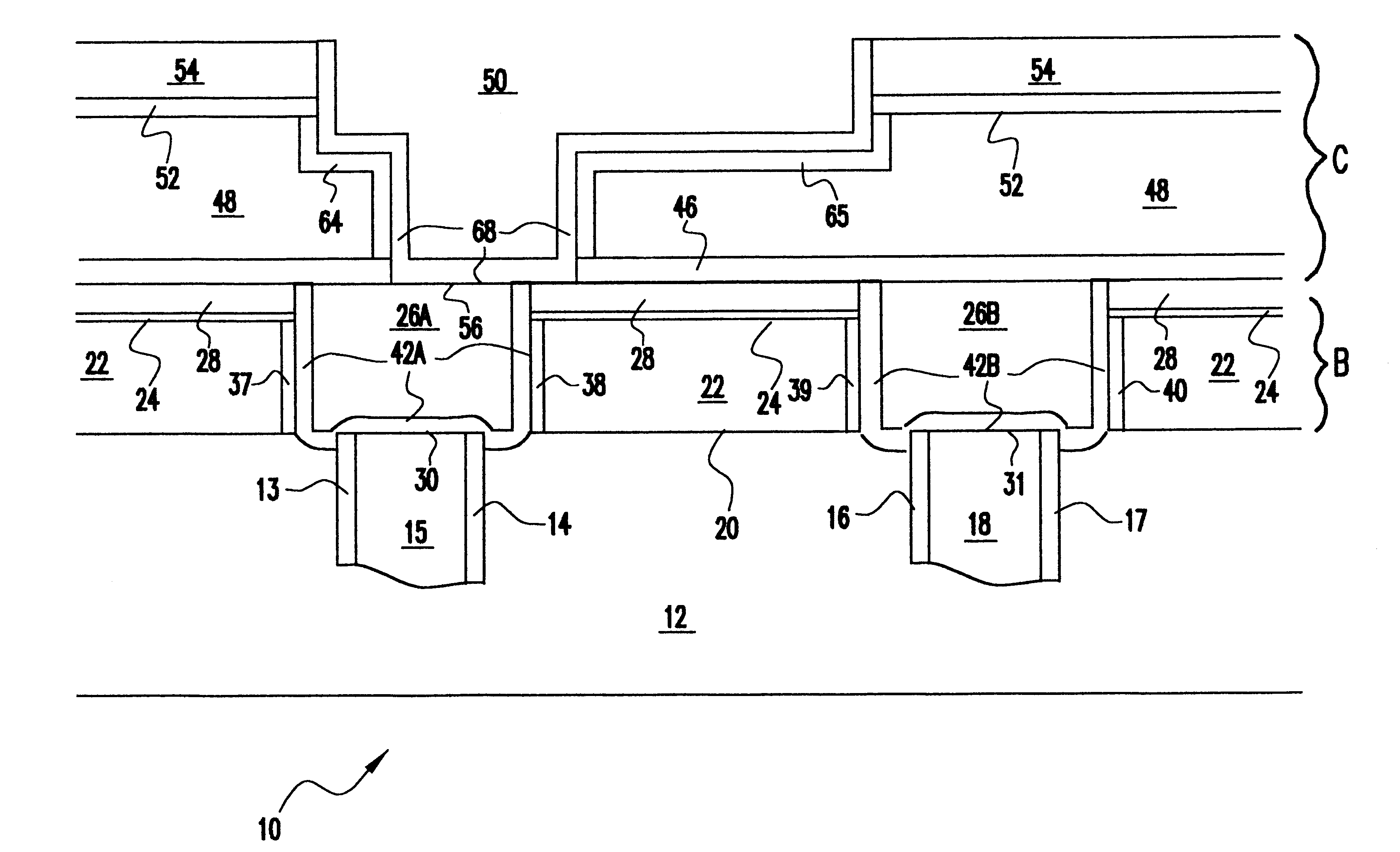
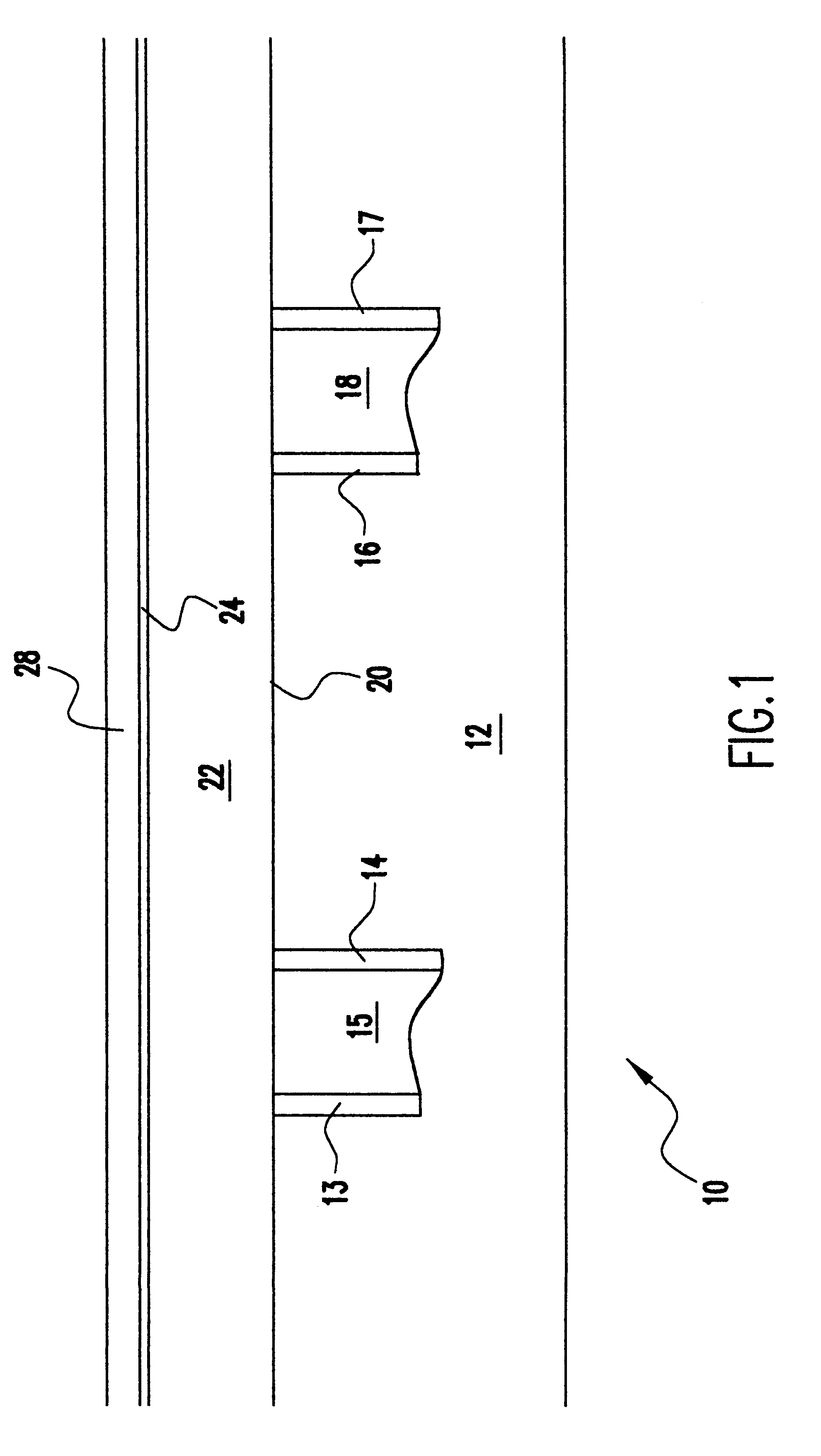
Referring now to FIG. 1, there is shown a cross-sectional view of an integrated circuit chip 10 having devices such as transistors, capacitors and underlying connections (not shown) formed thereon. At the bottom of the circuit chip is a substrate 12. The substrate is formed of Boron Phospho-Silicate Glass (BPSG) or Phospho-Silicate Glass (PSG). The substrate 12 defines exemplary stud walls 13 and 14 of a first stud 15 and stud walls 16 and 17 of a second stud 18. The studs are in communication with the underlying electrical connections. The number and location of the studs are determined as a matter of integrated circuit design and are unimportant to the practice of the invention in accordance with its basic principles. After a stud or plurality of studs are formed, a substrate surface 20 of the substrate 12 is planarized by a known method such as polishing, however other methods suitable to planarize a surface of a substrate can also be used.

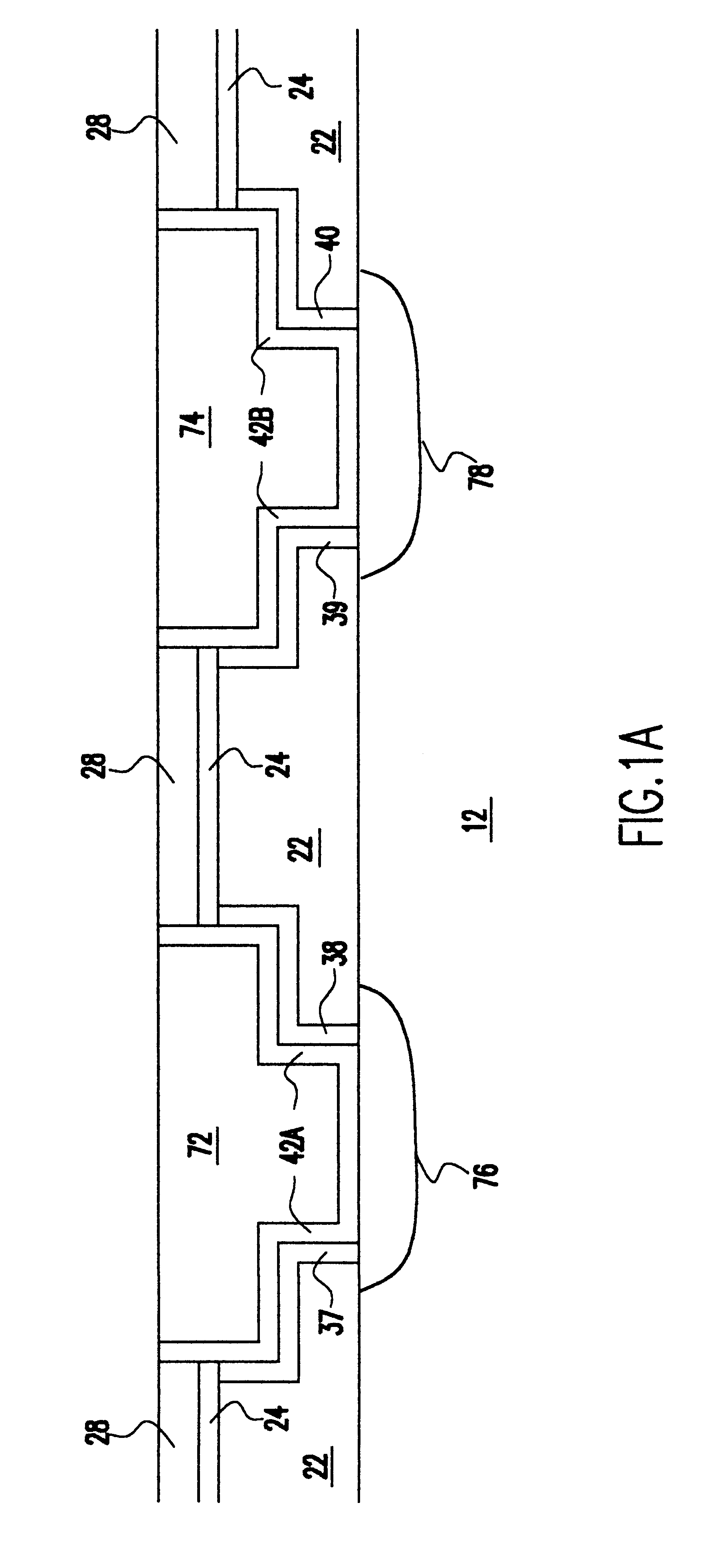
After the substrate surface 20 has been ...


PUM

PropertyMeasurementUnit
thickaaaaaaaaaa
thicknessaaaaaaaaaa
thicknessaaaaaaaaaa

Abstract

A method and structure for protecting a flowable oxide insulator in a semiconductor by oxidizing sidewalls of the FOX insulator, optionally nitridizing the oxidized FOX sidewalls, and then covering all surfaces of a trough or plurality of troughs in the FOX insulator, including the sidewalls, with a conductive secondary protective layer. In a multiple layer damascene structure, the surface of the FOX insulator is also oxidized, an additional oxide layer is deposited thereon, and a nitride layer deposited on the oxide layer. Then steps are repeated to obtain a comparable damascene structure. The materials can vary and each damascene layer may be either a single damascene or a dual damascene layer.

Description

1. Field of the InventionThe present invention generally relates to integrated circuit manufacturing and, more particularly, to the use of flowable oxide (FOX) layers as insulators or barriers for semiconductor devices and the protection of FOX layers from degradation in such applications.2. Description of the Prior ArtIncreases in both performance and manufacturing economy with increased integration density have led to the use of design rules with extremely small feature sizes and closeness of spacing in integrated circuit design. Reduced interconnection length between devices included in integrated circuits generally reduces signal propagation time and increases noise immunity. However, as integrated circuits are scaled to smaller design rules, reductions in wiring delays are diminished by increases in resistance (due to decreased cross-sectional area) and capacitance (due to increased connection proximity). This effect can only be ameliorated by reduced resistivity of conductors ...

Claims


Application Information

Patent Timeline
Patent Type & Authority Patents(United States)
IPC IPC(8): H01L21/02H01L21/768H01L21/70H01L21/311H01L21/316
CPCH01L21/31116H01L21/76807H01L21/76814H01L21/76826H01L21/76829H01L21/76831H01L21/7684H01L21/76843
Inventor GRECO, STEPHEN E.HUMMEL, JOHN P.LIU, JOYCEMCGAHAY, VINCENT J.MIH, REBECCASRIVASTAVA, KAMALESH
Owner INT BUSINESS MASCH CORP
Why Eureka
Try Eureka