Memory cell incorporating a chalcogenide element and method of making same

a memory cell and chalcogenide element technology, applied in semiconductor devices, diodes, electrical apparatuses, etc., can solve the problems of limited number of permissible logic states in such systems, electrical failure, and poor adhesion to silicon nitrid

Inactive Publication Date: 2001-05-22
ROUND ROCK RES LLC
View PDF4 Cites 731 Cited by
  • Summary
  • Abstract
  • Description
  • Claims
  • Application Information

AI Technical Summary

Problems solved by technology

The number of permissible logic states in such systems is limited generally only by the number of different resistance levels that may be reliably set in the programmable resistor.
There are several disadvantages associated with the present technique for incorporating a chalcogenide element.
To begin with, there is an inherent tendency for the chalcogenide stack to dislodge from the nitride layer, causing electrical failure.
This lifting problem is due to the rather poor adherence to silicon nitride exhibited by many chalcogenide materials.
Second, there are certain difficulties associated with the stack etch step.
Due to their physical and chemical nature, the etching of many chalcogenide materials is presently a process that is difficult to control.
Finally, the sheer number of masking steps required make the process relatively uneconomical.

Method used


Image

  • Memory cell incorporating a chalcogenide element and method of making same
  • Memory cell incorporating a chalcogenide element and method of making same
  • Memory cell incorporating a chalcogenide element and method of making same

Examples


Embodiment Construction

Conventional Process

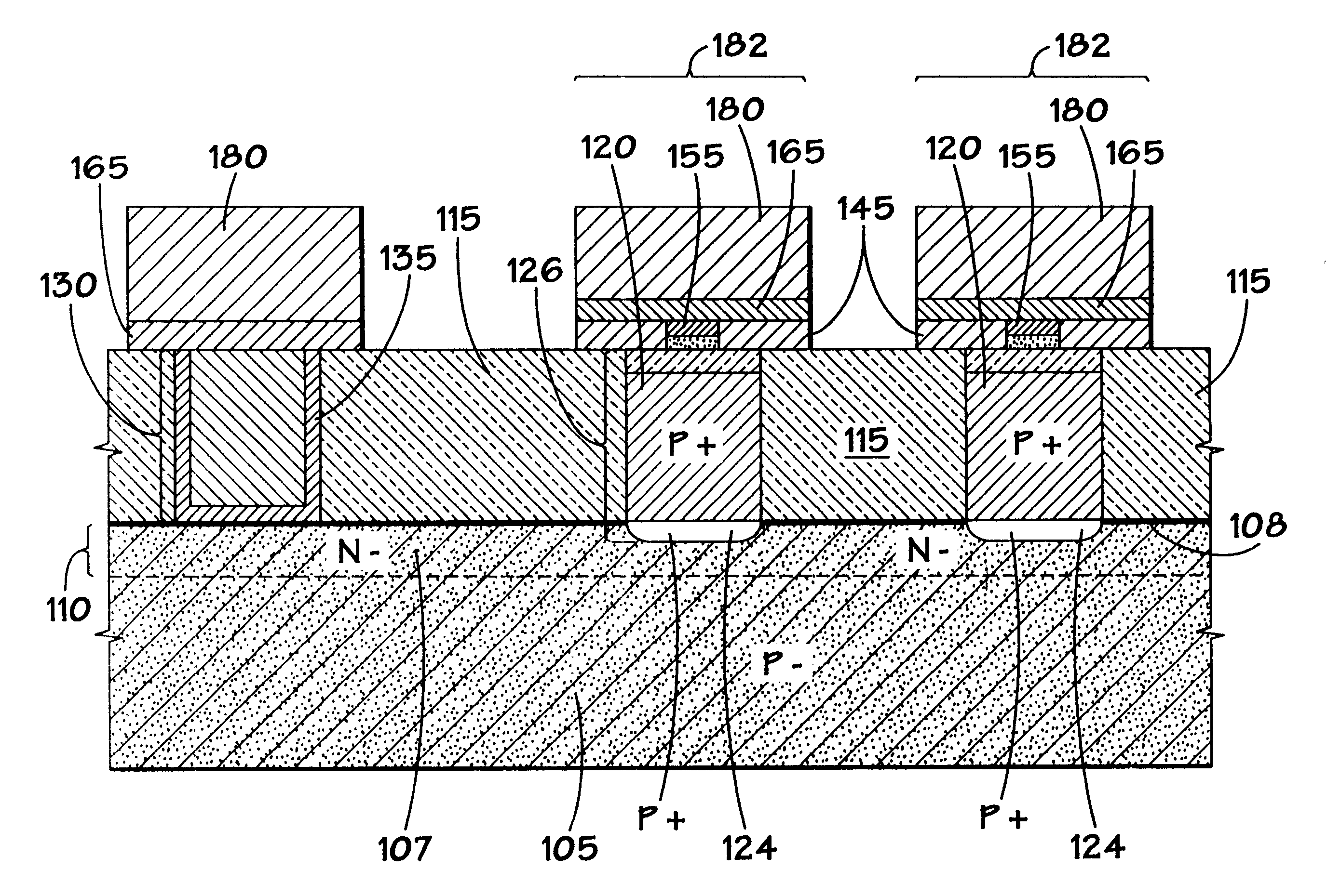
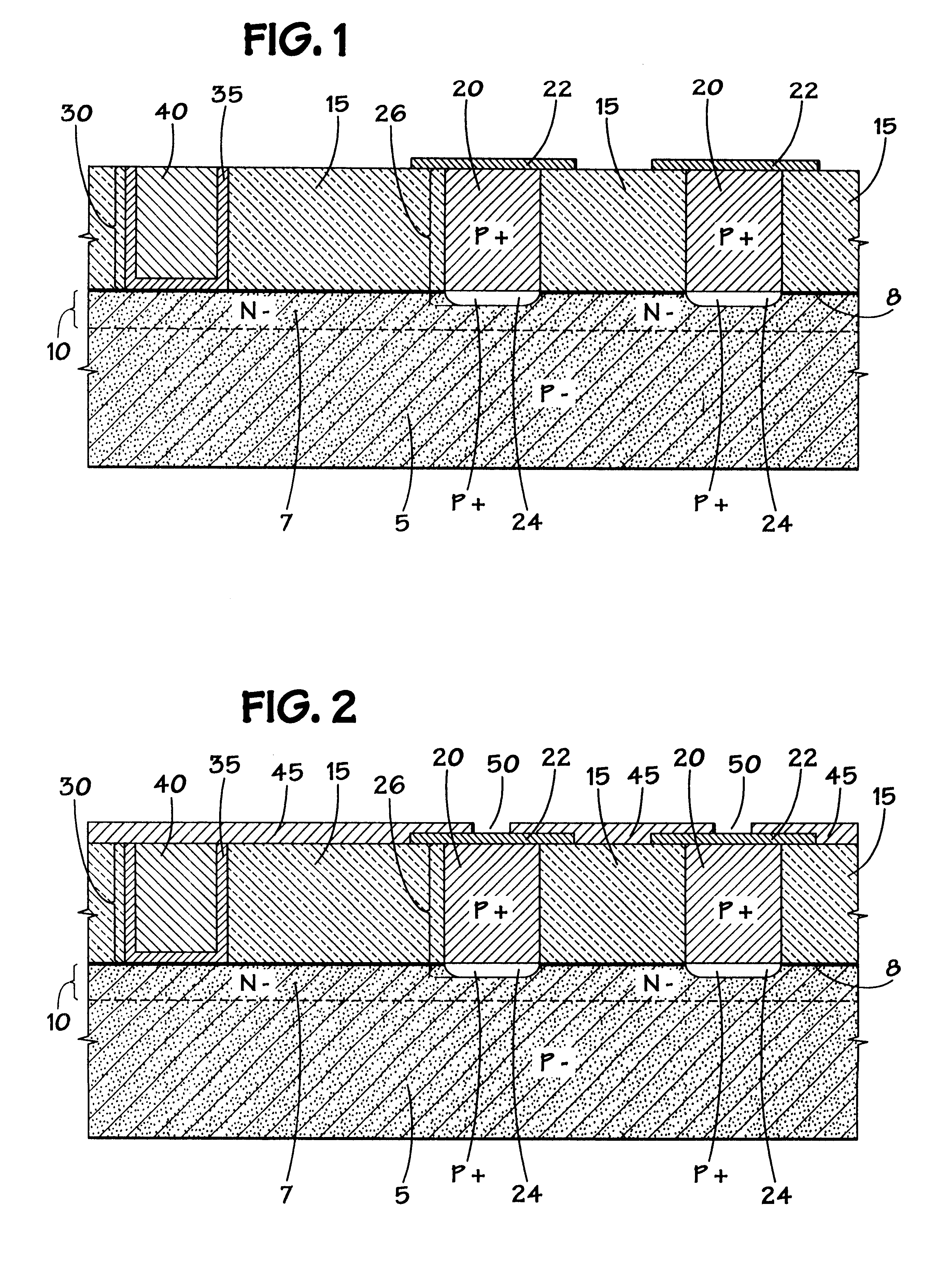
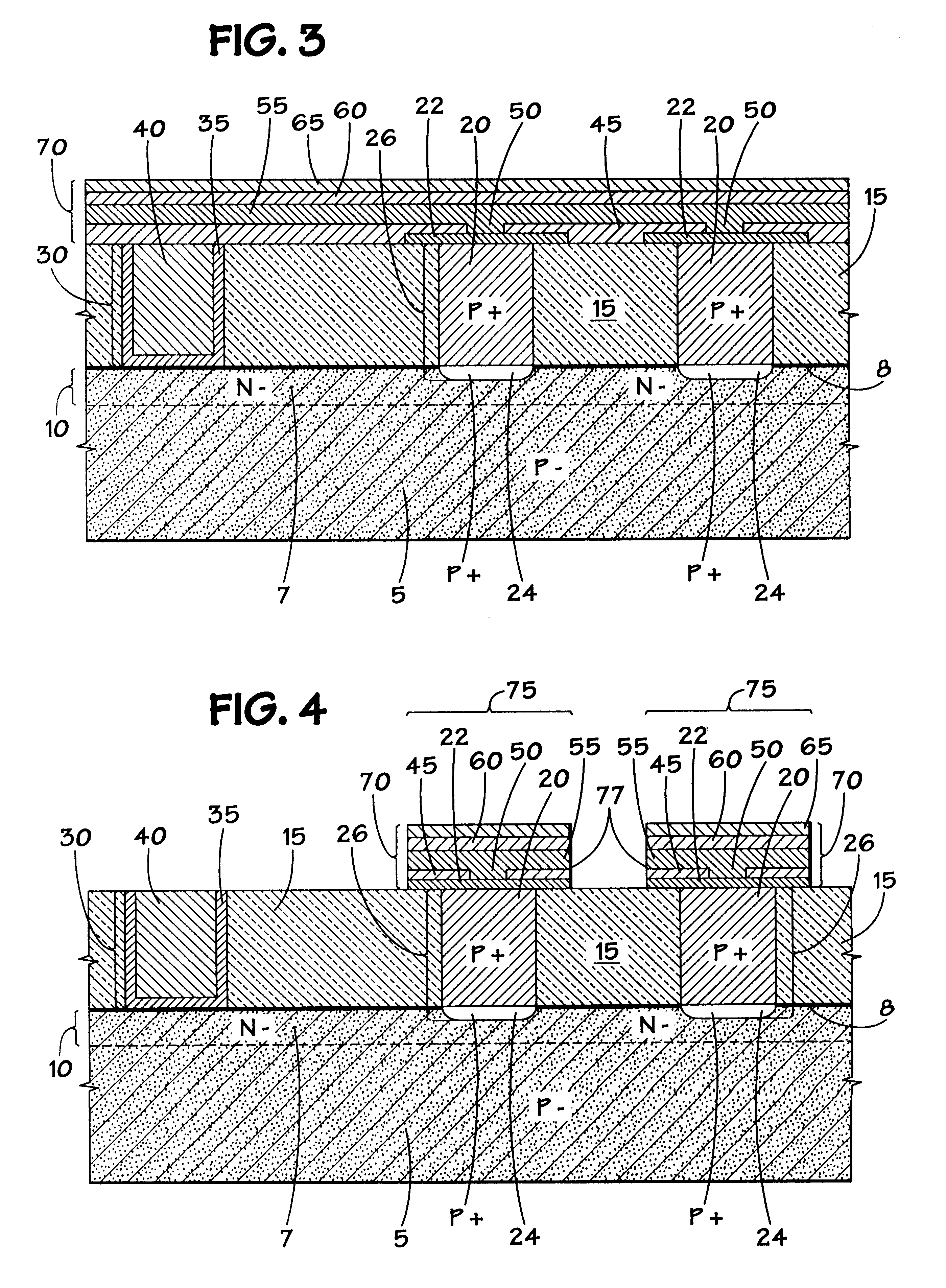
The embodiments are best described by first considering a common process currently practiced in a CMOS context to form a chalcogenide element. FIGS. 1-6 illustrate cross-sectional views of that existing process. FIG. 1 depicts a substrate 5 prior to the formation of the chalcogenide element. As a result of a number of preliminary processing steps, the substrate 5 includes n- doped regions 7 in the active area of the substrate 5, along with an optional layer of titanium silicide 8, that together function as a buried digit line 10. A relatively thick layer of silicon dioxide 15 overlies the buried digit lines 10. The silicon dioxide 15 has been masked with a contact pattern, not shown, and etched to create openings in which polycrystalline silicon plugs 20 are formed. A lower electrode 22, in the form of a layer of electrode material, such as carbon, overlies each plug 20. There are shallow p+ regions 24 extending below the plugs 20 as a result of diffusion of p+ m...


PUM

PropertyMeasurementUnit
thicknessaaaaaaaaaa
thicknessaaaaaaaaaa
thicknessaaaaaaaaaa

Abstract

A memory cell incorporating a chalcogenide element and a method of making same is disclosed. In the method, a doped silicon substrate is provided with two or more polysilicon plugs to form an array of diode memory cells. A layer of silicon nitride is disposed over the plugs. Using a poly-spacer process, small pores are formed in the silicon nitride to expose a portion of the polysilicon plugs. A chalcogenide material is disposed in the pores by depositing a layer of chalcogenide material on the silicon nitride layer and planarizing the chalcogenide layer to the silicon nitride layer using CMP. A layer of TiN is next deposited over the plugs, followed by a metallization layer. The TiN and metallization layers are then masked and etched to define memory cell areas.

Description

1. Field of InventionThis invention relates generally to semiconductor circuit devices and methods for making such devices. More particularly, this invention relates to semiconductor memory cells that incorporate a chalcogenide element and to methods for making chalcogenide memory cells.2. Description of the Related ArtA diode array is a well known memory system used in semiconductor memory devices. The individual diodes in a given array are typically addressed via digit and word lines. In previous diode array memory systems, the individual memory cells were limited to just two memory or logic states: high or low. However, the number of possible logic states for a given memory cell may be increased by connecting a programmable resistor in series with the selected diode. By selectively altering the resistance of the progammable resistor, the diode may be changed to different logic states that correspond to the changed resistance levels. The number of permissible logic states in such ...

Claims


Application Information

Patent Timeline
Patent Type & Authority Patents(United States)
IPC IPC(8): H01L21/70H01L21/285H01L21/768H01L21/02H01L21/8229H01L27/24H01L27/102
CPCH01L21/28512H01L21/76807H01L21/8229H01L27/1021H01L27/24H10B63/00H10B99/00
Inventor WOLSTENHOLME, GRAHAM R.GONZALEZ, FERNANDOZAHORIK, RUSSELL C.
Owner ROUND ROCK RES LLC
Why Eureka
Try Eureka