Single-electron floating-gate MOS memory

a floating gate and memory technology, applied in the field of single-electron floating gate mos memory, can solve the problems of inconvenient large-scale integration of structures, inability to precisely control the channel size, and the dimension of floating gates,

Inactive Publication Date: 2000-05-30
MINNESOTA RGT UNIV OF A CORP OF MN
View PDF10 Cites 274 Cited by
  • Summary
  • Abstract
  • Description
  • Claims
  • Application Information

AI Technical Summary

Benefits of technology

According to one aspect of the invention, the SEMM comprises a source-to-drain path with a channel region; a single floating gate for storing at least one charge carrier, the floating gate being disposed over the channel region and isolated from the channel region by a first gate dielectric layer; and a control gate disposed over the floating gate and isolated from the floating gate by a second gate dielectric layer so that a single charge carrier on the floating gate at room temperature produces a significant shift in threshold voltage of the channel region with respect to the control gate.
According to another aspect of the invention, the SEMM comprises a semiconductor source-to-drain path which includes a channel region; a single floating gate disposed over the channel region and isolated from the channel region by a first gate dielectric layer, the floating gate having dimensions less than 10 nanometers (nm) by 10 nanometers by 10 nanometers for storing a single charge carrier; and a control gate disposed over the floating gate and isolated from the floating gate by a second gate dielectric layer. The width of the source-to-drain path is smaller than the Debye screening length of the single charge carrier stored on the floating gate.
According to another aspect of the invention, the SEMM comprises a source-to-drain path including a channel region having a width of less than 70 nanometers; a single floating gate disposed over the channel region and isolated from the channel region by a first gate dielectric layer, the floating gate having dimensions less than 10 nanometers by 10 nanometers by 10 nanometers for storing a single charge carrier; and a control gate disposed over the floating gate and isolated from the floating gate by a second gate dielectric layer.
According to another aspect of the invention, the SEMM comprises a source-to-drain path including a channel region between a source and a drain, the channel region being a semiconductor, the channel region having a length from the source to the drain and also having a width; a floating gate for storing at least one charge carrier, the floating gate being disposed over the channel region and isolated from the channel region by a first gate dielectric layer, the floating gate having a width, wherein the width of the floating gate is self-aligned with the width of the channel; and a control gate disposed over the floating gate and isolated from the floating gate by a second gate dielectric layer.
According to another aspect of the invention, the SEMM comprises a source-to-drain path including a channel region between a source and a drain, the channel region being comprised of a semiconductor; a floating gate for storing at least one charge carrier, the floating gate being disposed over the channel region and isolated from the channel region by a first gate dielectric layer, the floating gate having lateral dimensions defined by lithography; and a control gate disposed over the floating gate and isolated from the floating gate by a second gate dielectric layer so that a single charge carrier on the floating gate at room temperature produces a significant shift in threshold voltage of the channel region with respect to the control gate.

Problems solved by technology

However, because this structure relies on the polysilicon grain structure of the source-to-drain path as the storage medium, it inherently prevents a precise control of the channel size, the floating gate dimension, and the tunnel barrier.
While both of these previous approaches strive to alleviate the challenges presented by nanofabrication (i.e., the fabrication of structures approaching the size of a nanometer), both rely on the use of statistically variant floating gate structures which lead to undesirable fluctuations in threshold voltage shifts and in the charging voltage, therefore making such structures unsuitable for large-scale integration.

Method used


Image

  • Single-electron floating-gate MOS memory
  • Single-electron floating-gate MOS memory
  • Single-electron floating-gate MOS memory

Examples


Embodiment Construction

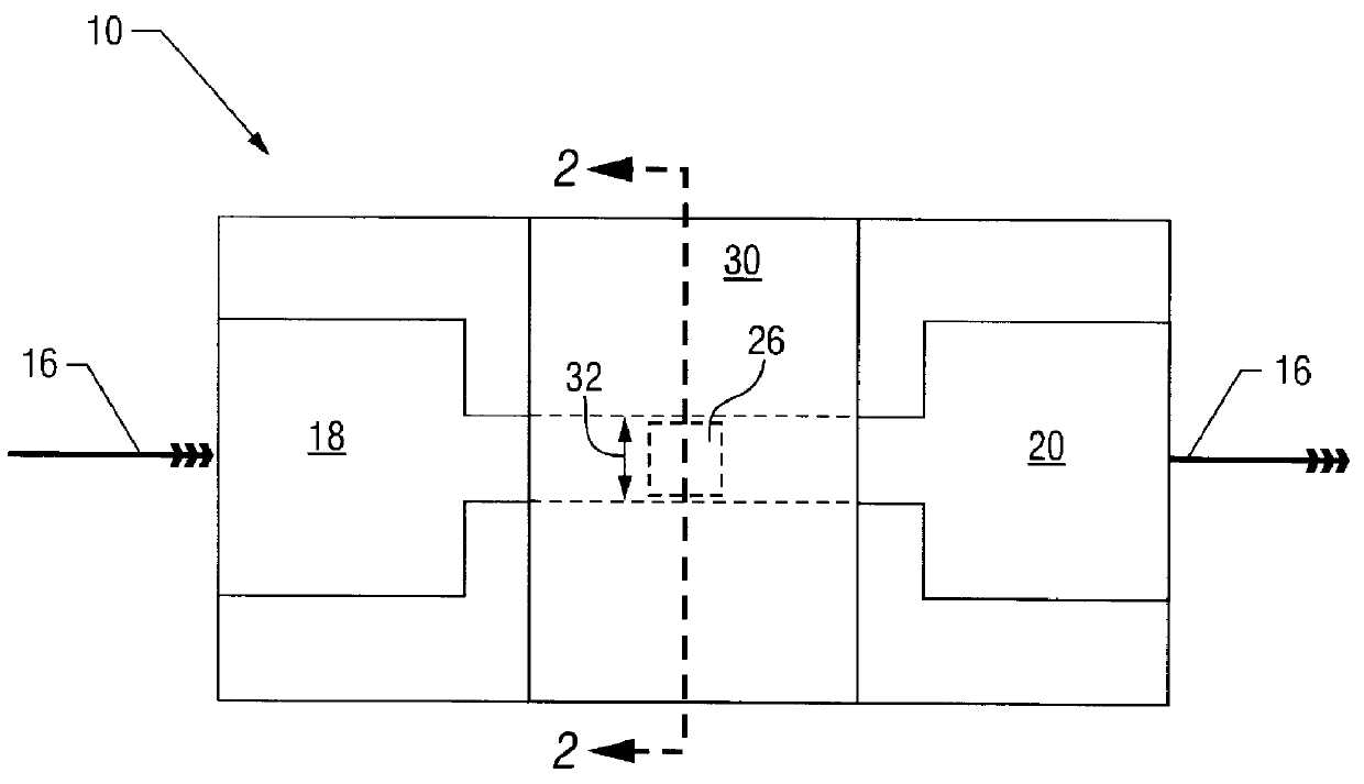
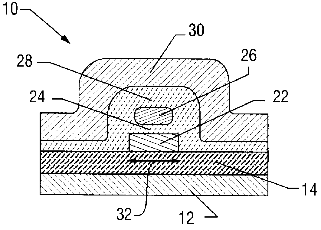
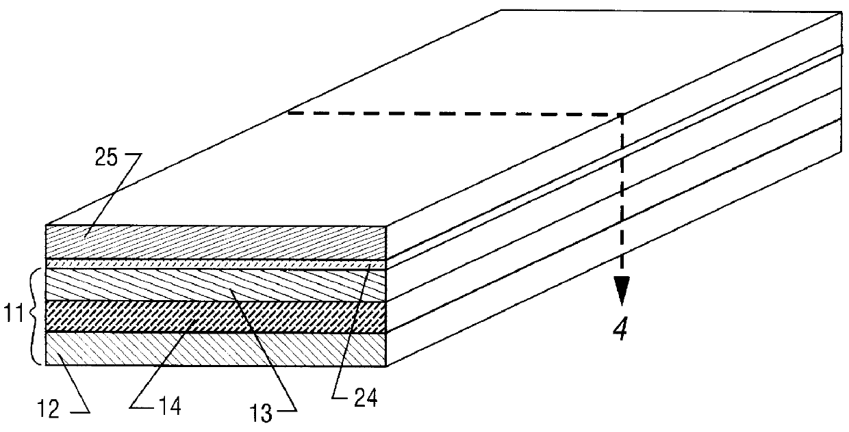
FIGS. 1 and 2 show the disclosed inventive SEMM 10. The SEMM is comprised of: a crystalline silicon substrate 12; a buried oxide layer 14; a source-to-drain path 16 including a source 18, a drain 20, and a channel region 22; a gate oxide 24; a nanoscale floating gate or "dot" 26; a control gate oxide 28; and a control gate 30.

The SEMM's channel width 32 is narrower than the Debye screening length of a single electron stored on the floating gate 26. Therefore, the storage of a single electron on the floating gate 26 is sufficient to screen the entire channel (i.e., the full channel width 32) from the potential (V.sub.cg) on the floating gate. The storage of a single electron produces a significant shift in the SEMM's threshold voltage.

The small floating gate 26 significantly increases the quantum energy of the electron stored on the floating gate, a necessary constraint for room-temperature operation. At the same time, the small capacitance of the gate oxide 24 relative to the contro...


PUM


Abstract

A Single Electron MOS Memory (SEMM), in which one bit of information is represented by storing only one electron, has been demonstrated at room temperature. The SEMM is a floating gate Metal-Oxide-Semiconductor (MOS) transistor in silicon with a channel width (about 10 nanometers) which is smaller than the Debye screening length of a single electron stored on the floating gate, and a nanoscale polysilicon dot (about 7 nanometers by 7 nanometers by 2 nanometers) as the floating gate which is positioned between the channel and the control gate. An electron stored on the floating gate can screen the entire channel from the potential on the control gate, and lead to: (i) a discrete shift in the threshold voltage; (ii) a staircase relation between the charging voltage and the shift; and (iii) a self-limiting charging process. The structure and fabrication of the SEMM is well adapted to the manufacture of ultra large-scale integrated circuits.

Description

II. TECHNICAL FIELDThis invention relates generally to a data storage device, and more specifically to a data storage device capable of representing a bit of information (i.e., a logic `0` or a logic `1`) by storing and detecting a single charge carrier during room-temperature operation.III. BACKGROUND OF THE INVENTIONTo increase the storage density of semiconductor memories, the size of memory cells must be reduced. Smaller memory cells also lead to faster speeds and lower power consumption.A widely-used semiconductor memory is the "floating gate" memory. A floating gate memory has a floating gate interposed between a channel and a control gate. Information is represented by storing a plurality of charges (e.g., hundreds of thousands) on the floating gate. The information stored in a floating gate memory can be determined because differing amounts of charge on the floating gate will shift the threshold voltage of the transistor. A relatively low threshold voltage (e.g., no excess c...

Claims


Application Information

Patent Timeline
Patent Type & Authority Patents(United States)
IPC IPC(8): H01L29/66H01L29/788
CPCB82Y10/00H01L29/7888Y10S977/937
Inventor CHOU, STEPHEN Y.GUO, LINGJIELEOBANDUNG, EFFENDI
Owner MINNESOTA RGT UNIV OF A CORP OF MN
Why Eureka
Try Eureka