Use of high-K dielectric material for ONO and tunnel oxide to improve floating gate flash memory coupling

a technology of tunnel oxide and dielectric material, which is applied in the direction of semiconductor devices, electrical apparatus, transistors, etc., can solve the problems of limiting the scaling down of the total physical thickness of the ono layer and the numerous challenges of the fabrication of the material layer within the device, so as to improve data retention and reliability, reduce the thickness of equivalent oxide, and improve the effect of coupling

Inactive Publication Date: 2003-09-09
MONTEREY RES LLC
View PDF13 Cites 271 Cited by
  • Summary
  • Abstract
  • Description
  • Claims
  • Application Information

AI Technical Summary

Benefits of technology

Thus, in the present invention, by use of a high-K dielectric material instead of silicon dioxide for the tunnel oxide layer, and at least one of the bottom oxide layer and the top oxide layer, a floating gate flash memory device may be fabricated having reduced dimensions without creation of interface states coming from contamination which could provide charge leakage paths within the modified ONO structure in the device. The present invention provides advantages such as (1) improved coupling between the control gate electrode and the floating gate electrode; (2) reduction of equivalent oxide thickness of the ONO structure; (3) improved data retention and reliability; and (4) the high-K dielectric material layer replacing the silicon dioxide layers allows fabrication of an ONO layer and a tunnel dielectric layer which are physically thicker, resulting in fewer charge leakage paths within these dielectric material layers. A variety of high-K or composite dielectric materials may be used for replacement of silicon dioxide in the in the tunnel dielectric layer and in the bottom and top oxide layers of a modified ONO structure. These dielectric materials may be formed in a nano-laminate, allowing for exact selection of composition, thickness and K value of the dielectric material layers. Thus, the present invention provides an advance in dielectric material layer fabrication technology for floating gate flash memory devices, and ensures proper dielectric separation of the control gate electrode from the floating gate electrode, and proper dielectric separation of the floating gate electrode from the channel, source and drain, while at the same time providing distinct process and economic advantages.

Problems solved by technology

However, as the ONO layer is made physically thinner, leakage current through the ONO layer may increase, which limits the scaling down of the total physical thickness of the ONO layer.
Numerous challenges remain in the fabrication of material layers within these devices.

Method used


Image

  • Use of high-K dielectric material for ONO and tunnel oxide to improve floating gate flash memory coupling
  • Use of high-K dielectric material for ONO and tunnel oxide to improve floating gate flash memory coupling
  • Use of high-K dielectric material for ONO and tunnel oxide to improve floating gate flash memory coupling

Examples


Embodiment Construction

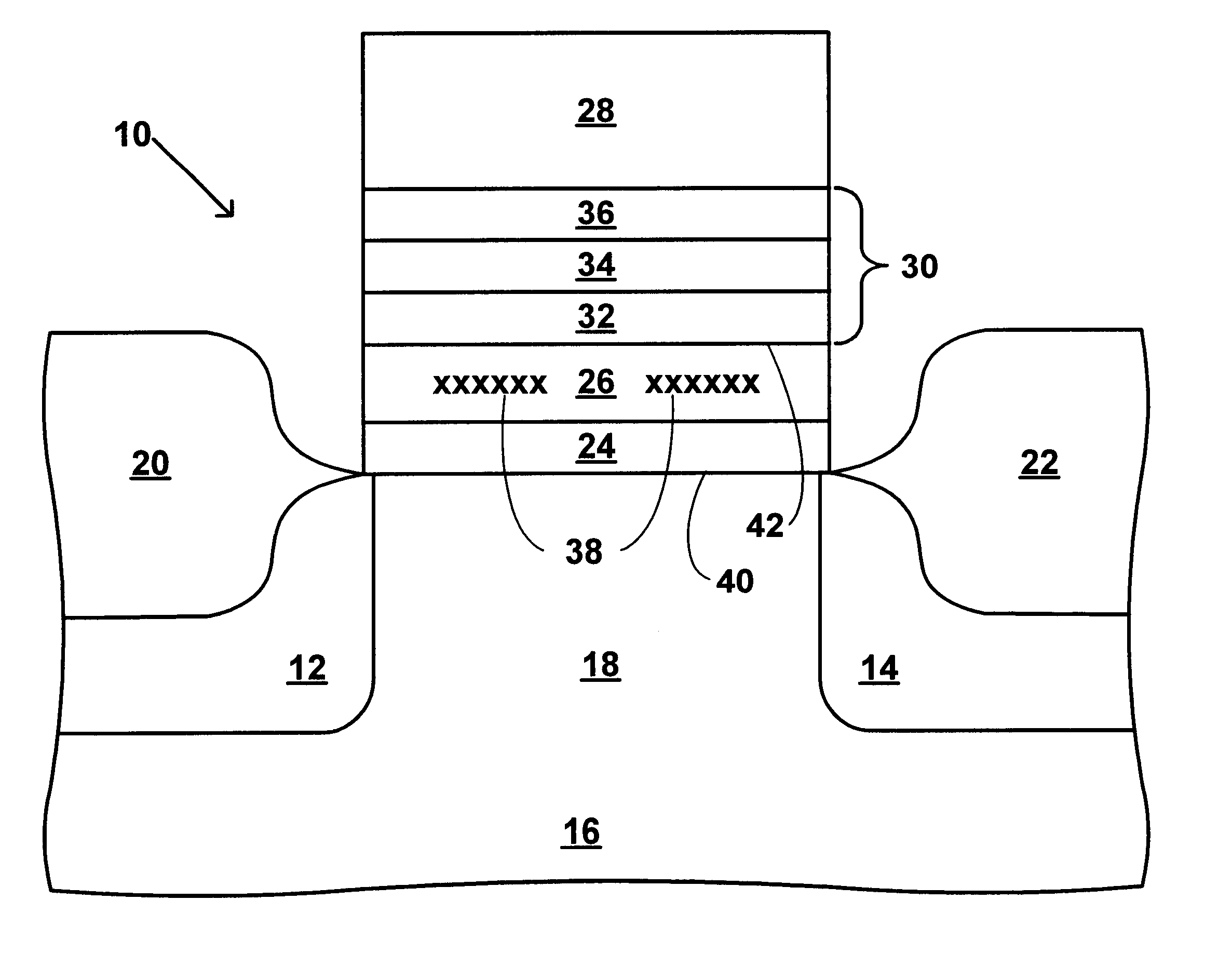
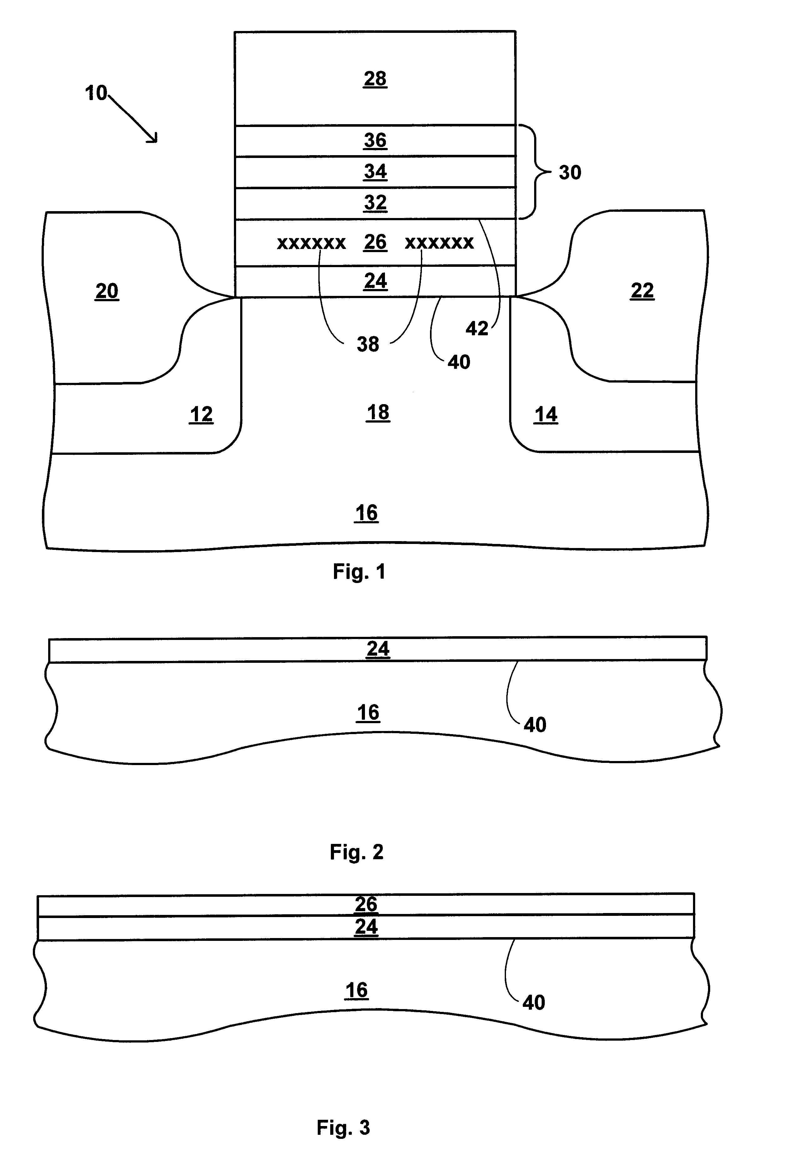
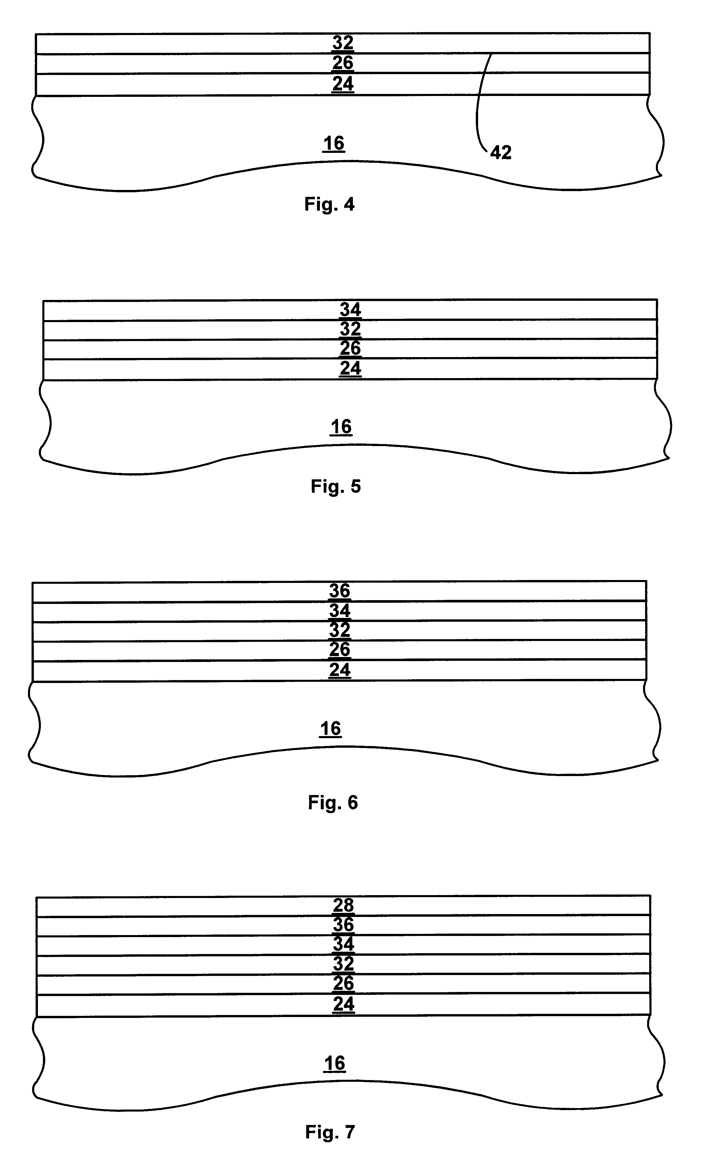
Referring first to FIG. 1, there is schematically shown in cross-section a floating gate flash memory device or cell 10 suitable for use in a floating gate flash EEPROM device. The cell 10 includes source / drain regions 12 and 14 located in a semiconductor substrate 16 and separated by a channel region 18. First and second bit line oxide regions 20 and 22 overlie source / drain regions 12 and 14, respectively. A tunnel dielectric material layer 24 overlies the channel region 18. A floating gate electrode 26 overlies the tunnel dielectric material layer 24. In one embodiment, the tunnel dielectric material layer 24 comprises a high-K dielectric material. In another embodiment, the tunnel dielectric material layer 24 is a composite dielectric material, comprising a mixture of a standard-K dielectric material, such as silicon dioxide, silicon nitride, silicon oxynitride or aluminum oxide, with a high-K dielectric material, such as, for example, hafnium oxide or zirconium oxide.

Referring s...


PUM


Abstract

A floating gate flash memory device including a substrate comprising a source region, a drain region, and a channel region positioned therebetween; a floating gate electrode positioned above the channel region and separated from the channel region by a tunnel dielectric material layer; and a control gate electrode positioned above the floating gate electrode and separated from the floating gate electrode by an interpoly dielectric layer, the interpoly dielectric layer comprising a modified ONO structure having a bottom dielectric material layer adjacent to the floating gate electrode, a top dielectric material layer adjacent to the control gate electrode, and a center layer comprising a nitride and positioned between the bottom dielectric material layer and the top dielectric material layer, in which the tunnel dielectric material layer, and at least one of the bottom dielectric material layer and the top dielectric material layer, comprise a high-K dielectric material.

Description

The present invention relates to a structure and a process for fabrication of a semiconductor device including a high-K dielectric material for a tunnel dielectric and in a modified ONO structure, in particular to a structure and process for fabrication of a floating gate flash memory device.Non-volatile memory devices are currently in widespread use in electronic components that require the retention of information when electrical power is terminated. Non-volatile memory devices include read-only-memory (ROM), programmable-read-only memory (PROM), erasable-programmable-read-only memory (EPROM), and electrically-erasable-programmable-read-only-memory (EEPROM) devices. EEPROM devices differ from other non-volatile memory devices in that they can be electrically programmed and erased. Flash EEPROM devices are similar to EEPROM devices in that memory cells can be programmed and erased electrically. However, flash EEPROM devices enable the erasing of all memory cells in the device using...

Claims


Application Information

Patent Timeline
Patent Type & Authority Patents(United States)
IPC IPC(8): H01L21/02H01L21/28H01L29/51H01L21/336H01L29/66H01L29/40H01L29/788
CPCH01L21/28194H01L21/28273H01L29/513H01L29/66825H01L29/7883H01L29/517H01L29/518H01L29/40114
Inventor WANG, ZHIGANGGUO, XINHE, YUE-SONG
Owner MONTEREY RES LLC
Why Eureka
Try Eureka