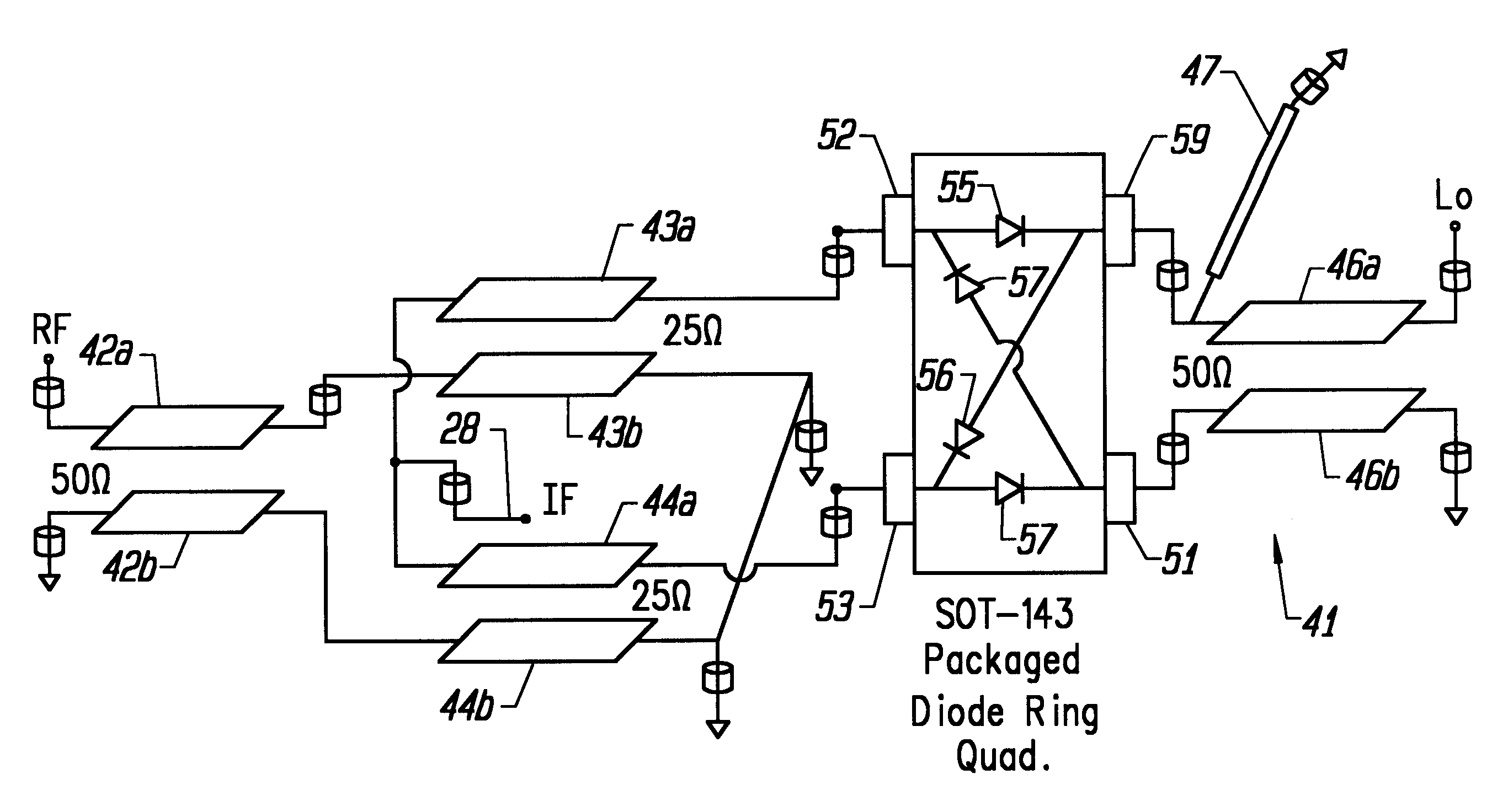
Multi-layer printed wiring board having integrated broadside microwave coupled baluns
a multi-layer printed and microwave coupled technology, applied in waveguides, waveguide type devices, high frequency circuit adaptations, etc., can solve the problems of incompatibility with printed wiring boards and relatively high prior art baluns
- Summary
- Abstract
- Description
- Claims
- Application Information
AI Technical Summary
Benefits of technology
Problems solved by technology
Method used
Image
Examples
Embodiment Construction
)
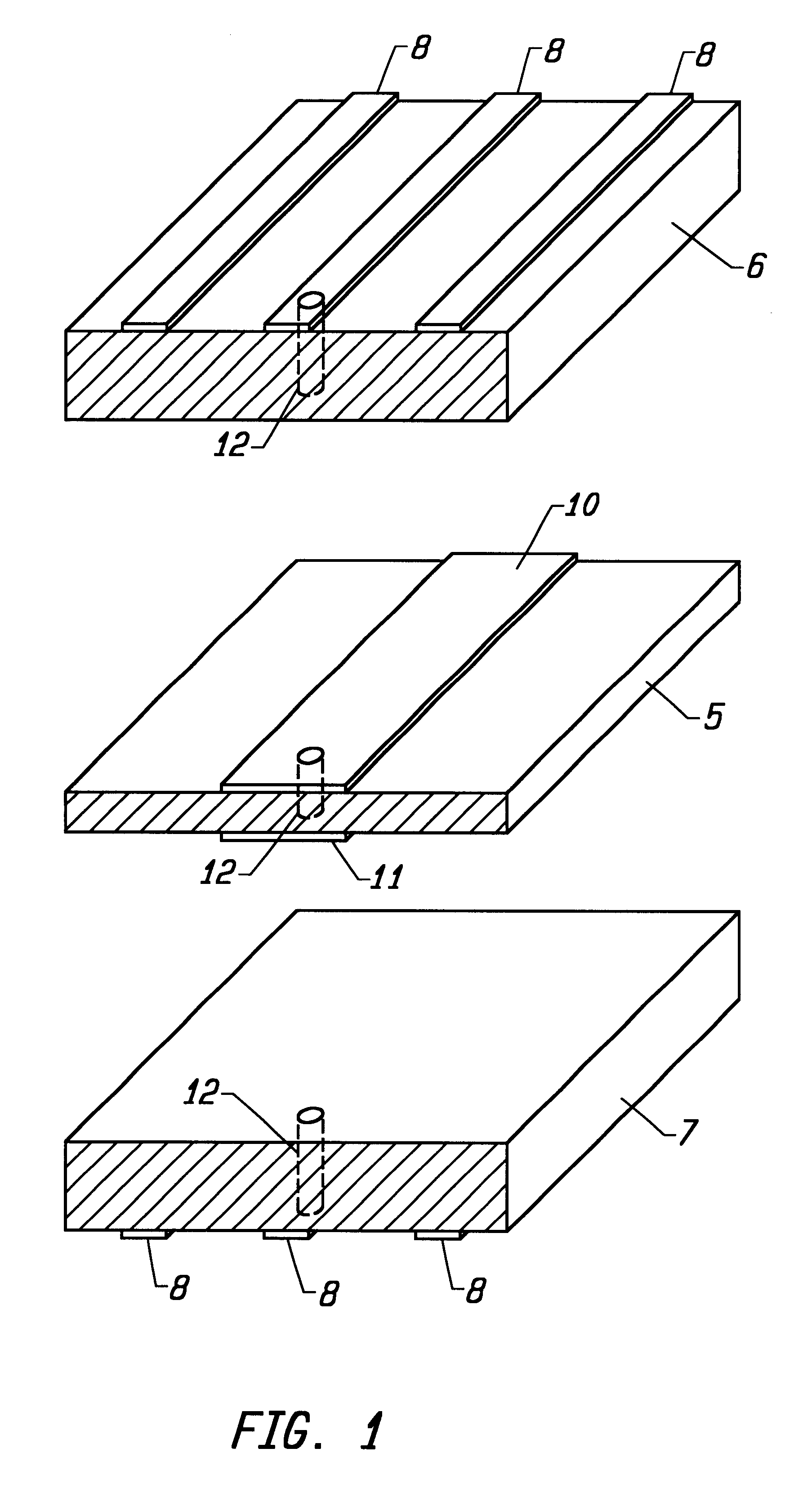
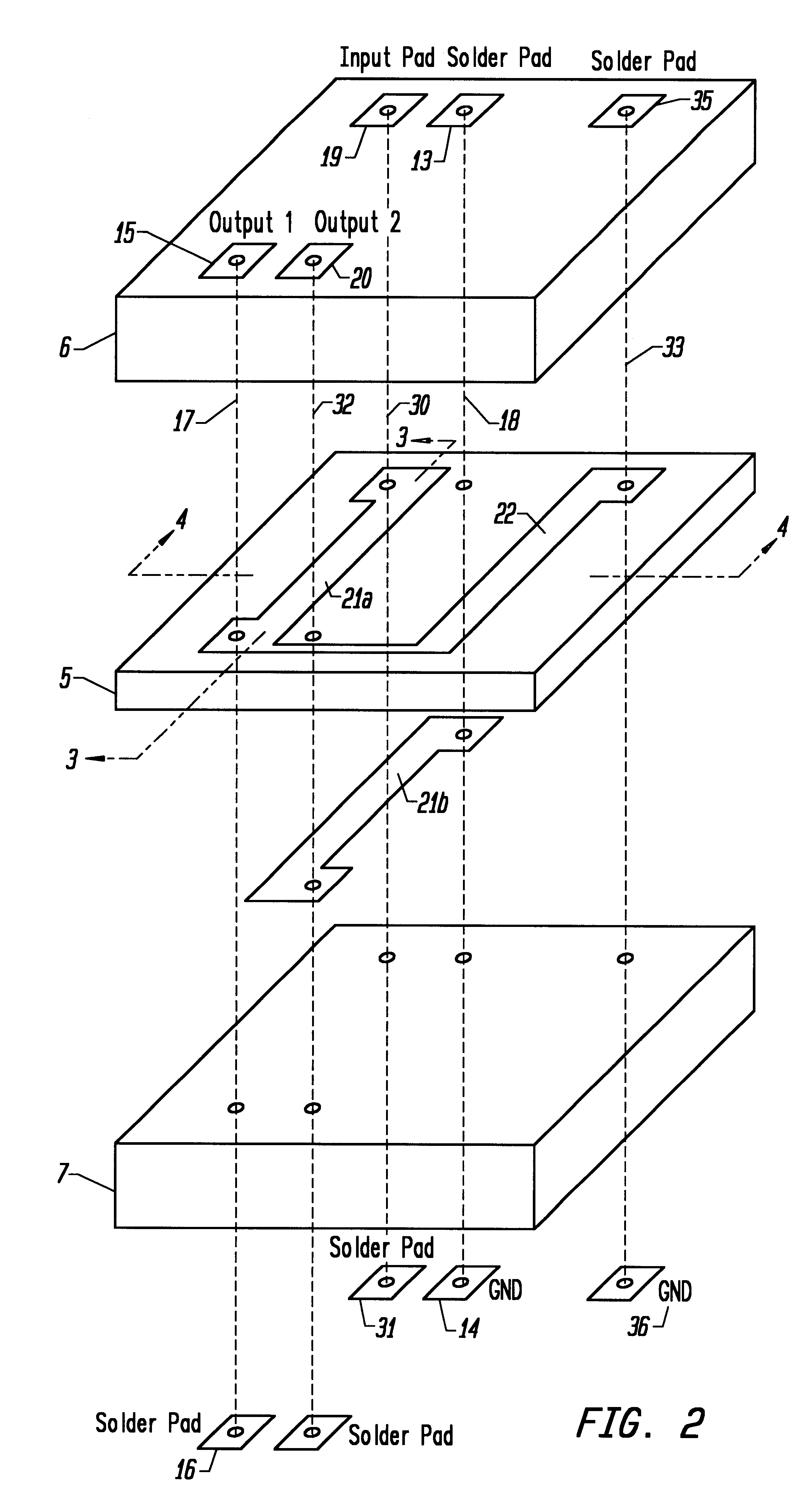
Referring to FIG. 1 there is shown in simplified form to illustrate the building blocks of a further structure, a multi-layer printed wiring board having a dielectric layer 5 sandwiched between first and second outer insulating layers 6 and 7 to form a multi-layer structure. To form an embedded broadside coupled balun (which is described in detail below) the outer surfaces of said first and second outer insulating layers are provided with conductive films 8 which may be selectively etched to form interconnects for connecting circuit components mounted on the surface of the printed board to the structure embedded in the board. In accordance with the present invention, thin elongated conductors 10 and 11 are formed on the opposite surfaces of the center layer of dielectric material 5. The broadsides of the elongated conductors 10 and 11 are directly opposite one another for broadside coupling. These conductors may be formed by the additive process in which the conductors are formed b...
PUM
 Abstract
Description
Claims
Application Information


