Micro-electro-mechanical optical device

a micro-electromechanical and optical device technology, applied in the direction of snap-action arrangements, instruments, sheets/panels, etc., can solve the problems of limiting the size the angle of rotation of the optical device, and the typical range of motion of the optical device perpendicular to the substra

Inactive Publication Date: 2001-07-24
AVAGO TECH WIRELESS IP SINGAPORE PTE +1
View PDF2 Cites 21 Cited by
  • Summary
  • Abstract
  • Description
  • Claims
  • Application Information

AI Technical Summary

Problems solved by technology

However, the typical range of motion for the optical device perpendicular to the substrate is limited to the thicknesses of the material layers.
In particular, such a limited range of motion for the optical devices also limits the size of the optical device, the angle of rotation for the optical device, or both.

Method used


Image

  • Micro-electro-mechanical optical device
  • Micro-electro-mechanical optical device
  • Micro-electro-mechanical optical device

Examples


example 2

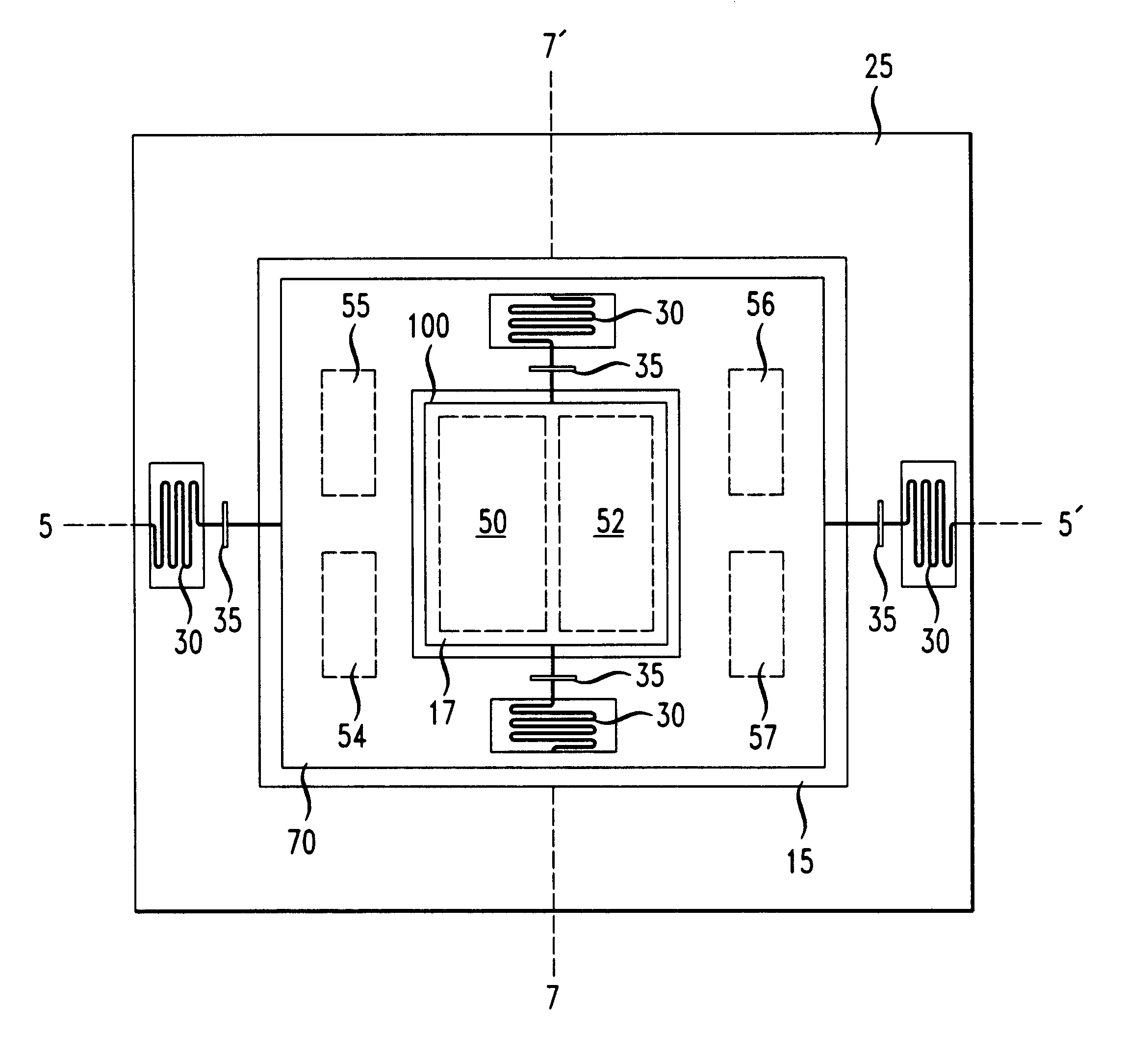
A micro-electro-mechanical optical device having the structure depicted in FIG. 5 was formed. The electromechanical optical device was formed on a surface of a silicon substrate. The silicon substrate had six 0.5 .mu.m thick POLY0 pads 50, 52, 54, 55, 56 and 57 on regions thereof. The micro-electro-mechanical optical device was formed with the fabrication steps described in Example 1. The optical device was lifted above the surface of the substrate to a substantially planar orientation with respect to the substrate surface as described in Example 1.

A voltage of about 100 V was applied between the optical device and pads 50, 55, and 56, underlying the optical device 17 on the substrate surface. When the voltage was applied between the optical device and pads 50, 55, and 56 the optical device pivoted about axis 7--7' and axis 5--5' (FIG. 5), so that the optical device was tilted an angle of about 5.degree. with respect to the substrate surface so that the corner denoted as 100 was the...


PUM


Abstract

A method for pivoting an optical device about one or more axes thereof is disclosed. Springs couple the optical device to the micro-electro-mechanical structure. A portion of the springs are fastened on the micro-electro-mechanical structure. Fastening the portion of each spring on the electromechanical structure prevents the springs from moving the optical device in a translational direction when such optical device pivots about the one or more axes.

Description

The present invention relates generally to optical communication systems and more particularly, to micro-electro-mechanical optical devices.DESCRIPTION OF THE RELATED ARTOptical communication systems typically include a variety of optical devices (e.g., light sources, photodetectors, switches, attenuators, mirrors, amplifiers, and filters). The optical devices transmit, modify, or detect optical signals in the optical communications systems. Some optical devices are coupled to micro-electro-mechanical structures (e.g., thermal actuators) forming a micro-electro-mechanical optical device. The term micro-electro-mechanical structure as used in this disclosure refers to a structure that moves mechanically under the control of an electrical signal. The microelectro-mechanical structure moves the optical devices from a first position to a second position.Typically, both the micro-electro-mechanical structure and the optical device are fabricated by patterning a plurality of material laye...

Claims


Application Information

Patent Timeline
Patent Type & Authority Patents(United States)
IPC IPC(8): B81B3/00G02B26/08F16S1/02B81B5/00B81B7/00
CPCB81B3/004B81B3/0062G02B26/0866G02B26/0841B81B7/0003B81B2201/042
Inventor AKSYUK, VLADIMIR ANATOLYEVICHBISHOP, DAVID JOHN
Owner AVAGO TECH WIRELESS IP SINGAPORE PTE
Why Eureka
Try Eureka