Method and apparatus for testing chips

a technology of chips and apparatus, applied in electrical equipment, electrical testing, instruments, etc., can solve the problems of reject chips, faulty chips, and high cost of assembly-ready chips,

Inactive Publication Date: 2001-08-21
PAC TECH PACKAGING TECH
View PDF10 Cites 12 Cited by
  • Summary
  • Abstract
  • Description
  • Claims
  • Application Information

AI Technical Summary

Benefits of technology

As a result, it becomes clear that the electrical testing of the wiring structure of the substrate during its manufacturing process is not linked with an additional processing step. Rather, as a result of the method in accordance with the invention, an almost inherent quality test is made possible during a manufacturing step which is necessary in any case. In addition, the electrical checking of the wiring structure of the substrate takes place before its completion by means of a final encasing, or before the production of a final contacting in the flip-chip method, so that the further processing of substrates with defective wiring structures is avoided.
It has turned out to be advantageous for the configuring of a wettable bond-pad metallization if the latter exhibits a gold or palladium alloy.

Problems solved by technology

Apart from the costs that are caused by the manufacturing of the wafer, the costs for the manufacturing of an assembly-ready, packaged chip are primarily caused by the subsequent manufacturing steps.
These steps are primarily the creation of so-called bumps on the bond pads of the chips, which are created from the wafer by singling them out, and the expensive packaging of the chips.
Many times, however, the causes for the malfunctioning of a chip have their base in one of the manufacturing steps which precede the packaging of the chip, so that faulty chips which represent rejects even before the encasing, are packaged unnecessarily.
As a result, the costs associated with what will be a reject in any case are increased even further.
Overall, the processing of chips or complete wafers by means of the flip-chip method leads to complex structures which do not allow for the complete testability of individual chips or complete wafers under defined test conditions, such as are prescribed for a burn-in test, for example, without risk to the entire structure when using known test methods.
While it is indeed known in the art to check individual chips or even complete wafers with appropriate test devices before carrying out a subsequent connecting technique, a quality check of such a type can only be carried out, however, with exceptional effort, which is in addition to the carrying out of the connecting technique which is already complex in itself.

Method used


Image

  • Method and apparatus for testing chips
  • Method and apparatus for testing chips
  • Method and apparatus for testing chips

Examples


Embodiment Construction

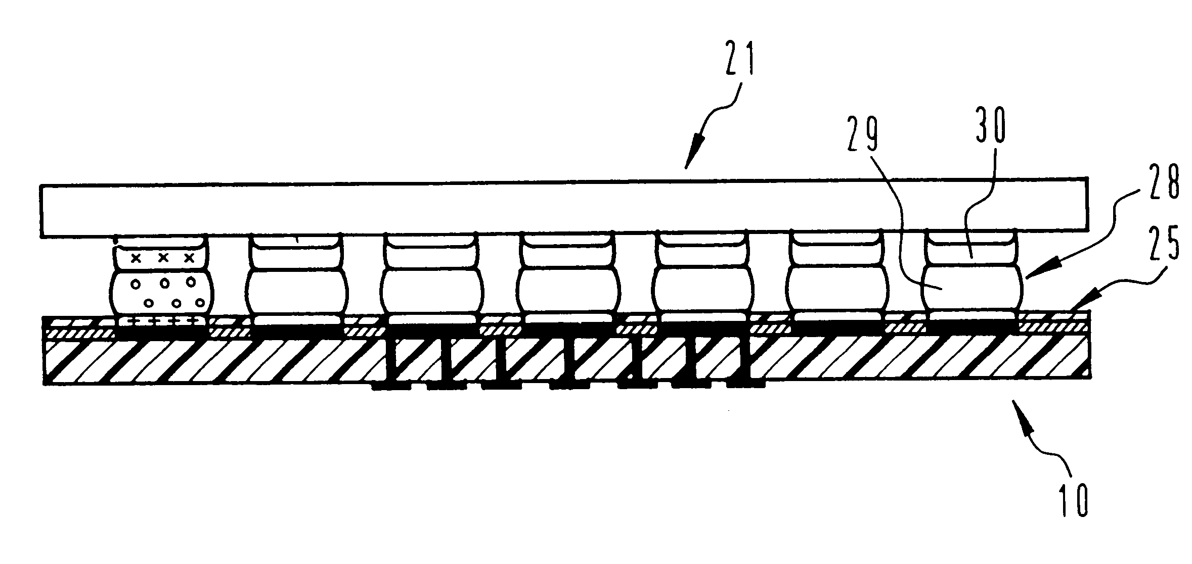
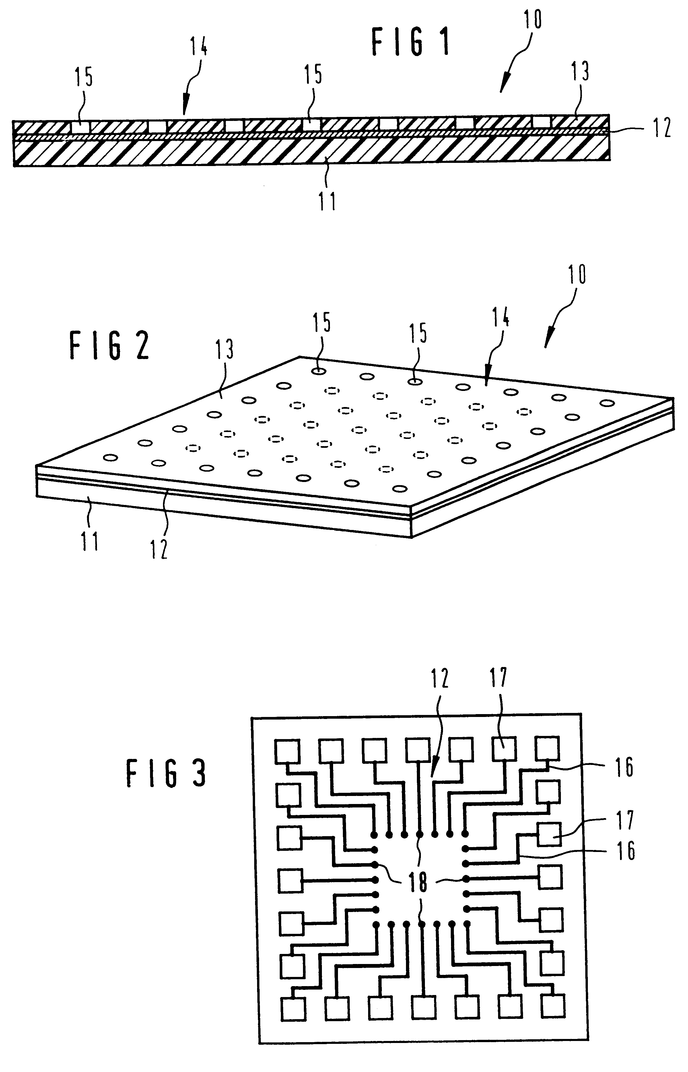
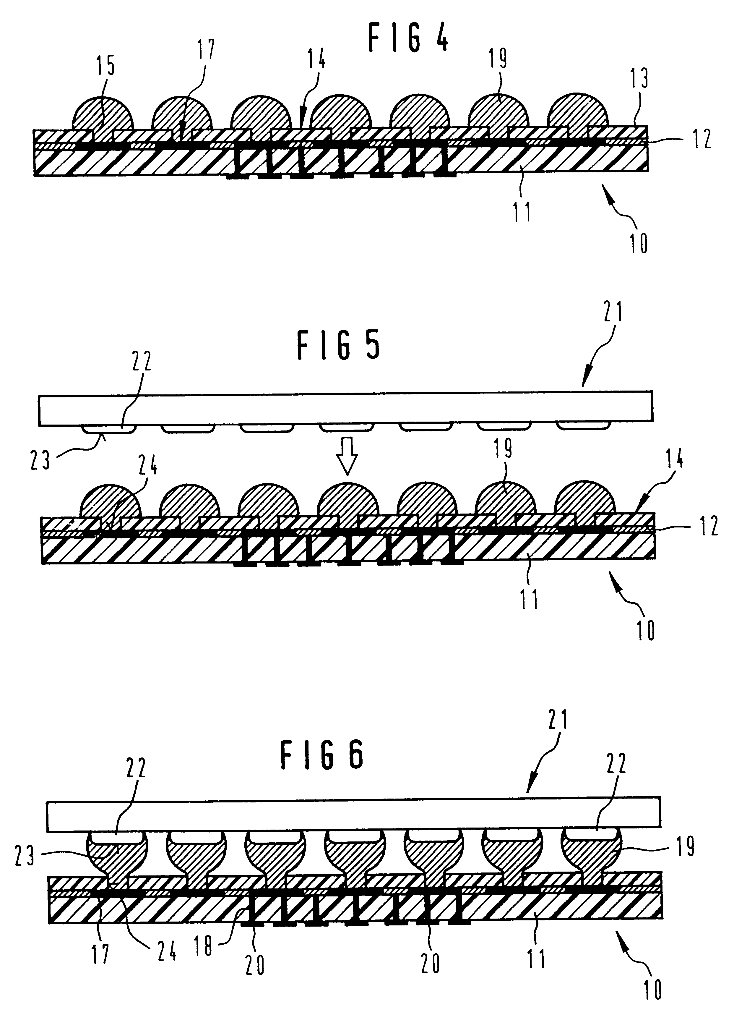
FIG. 1 shows a solder-deposit carrier 10 with a carrier layer 11 and an electrically conductive coating which is applied to the carrier layer 11 and which is configured here as a structured metallization in the form of a wiring structure 12. Located on the wiring structure 12 is a photo-sensitive polymer layer 13, which is structured in the manner shown by means of a photo-lithographic process that is known in the art in order to form a transfer mask 14, and which exhibits mask openings 15.

FIG. 2 shows the transfer mask 14 with the mask openings 15 in a top view. Along with the mask openings 15, which are placed in continuous lines parallel to the circumference of the solder-deposit carrier 10 and which correspond in their placement to the conventional input / output contact pad arrangement of a chip, there are additional mask openings 15 drawn in, which are distributed uniformly over the inner region of the polymer layer 13 of the embodiment shown in FIG. 2, which are shown by means ...


PUM


Abstract

Method and apparatus for the testing of substrates which are provided with a wiring structure, in particular, chips (21), in conjunction with which, by means of a solder-deposit carrier (25) which is provided with a structured, electrically conductive coating (12) with bond pads (17) for the arranging of solder deposits (28) and their transfer to correspondingly arranged bond pads (22) of a substrate (21), an electrical check of the wiring structure of the substrate (21) takes place during the transfer of the solder deposits (28).

Description

1. Field of the InventionThe present invention pertains to a method for testing a substrate which is provided with a wiring structure, in particular, a chip in accordance with the introductory clause of claim 1, a solder-deposit carrier in accordance with the introductory clause of claim 11 which can be used with this method, and a solder deposit in accordance with the introductory clause of claim 19, which can be used on the solder-deposit carrier.2. Discussion of the Related ArtThe manufacture of an IC that is assembly-ready, such as is used in electronic devices for EDP for example, is divided into a large number of manufacturing steps from a wafer to an encased, assembly-ready chip.Apart from the costs that are caused by the manufacturing of the wafer, the costs for the manufacturing of an assembly-ready, packaged chip are primarily caused by the subsequent manufacturing steps. These steps are primarily the creation of so-called bumps on the bond pads of the chips, which are cre...

Claims


Application Information

Patent Timeline
Patent Type & Authority Patents(United States)
IPC IPC(8): G01R1/073H01L21/48H01L21/02G01R31/02G01R31/26H01L21/66
CPCG01R1/07307H01L21/4853H01L2924/01322H01L2224/16225H01L2924/15173H01L2224/11003H01L2224/05573H01L2224/05568H01L2224/06131
Inventor ZAKEL, ELKEANSORGE, FRANKKASULKE, PAULOSTMANN, ANDREASASCHENBRENNER, ROLFDIETRICH, LOTHAR
Owner PAC TECH PACKAGING TECH
Why Eureka
Try Eureka