Electronic sub-assembly and method for the production of an electronic sub-assembly

a technology of electronic sub-assembly and sub-assembly, which is applied in the direction of basic electric elements, electrical apparatus, and association of printed circuit non-printed electric components, can solve the problems of loss of positioning accuracy, and achieve the effects of preventing any slippage during further processing, low thermal resistance, and loss of positioning accuracy

Active Publication Date: 2019-03-12
SCHWEIZER ELECTRONIC
View PDF24 Cites 4 Cited by
  • Summary
  • Abstract
  • Description
  • Claims
  • Application Information

AI Technical Summary

Benefits of technology

[0006]During the later lamination process this layer can, however, become soft again, which might result in the loss of positioning accuracy. In order to prevent this, according to the invention, a “shadow mask” or hole mask, which is to be introduced into the layered structure, is provided as the next layer, which shadow mask will serve as a “template”, holding the component in its position during the pressing or lamination. This layer comprises at least one recess whose dimensions are determined by the component to be received such that the recess will enclose the component tightly, preventing any slippage during further processing. In addition, this layer is used for creating a low-resistance heat sink path, as well as for providing a low-ohmic connection from the component to the high-current path.
[0007]This allows building a symmetrical layer structure so that the at least one component is embedded in a sequence of layers that is identical “upwards” and “downwards”. Correlating layers can each have equal dimensions so that differences in tension between the areas “above” and “below” the component are mostly excluded. This will prevent thin components (semiconductors) from warping.
[0009]The fact that the at least one component has been inserted into a sheet metal layer of essentially the same thickness, which layer surrounds the component completely, will additionally result in low thermal resistance at high thermal capacity.
[0010]Furthermore, the elimination of a connecting point (i.e., solder, sinter, or gluing location) below the component will considerably reduce the vulnerability.

Problems solved by technology

During the later lamination process this layer can, however, become soft again, which might result in the loss of positioning accuracy.

Method used


Image

  • Electronic sub-assembly and method for the production of an electronic sub-assembly
  • Electronic sub-assembly and method for the production of an electronic sub-assembly
  • Electronic sub-assembly and method for the production of an electronic sub-assembly

Examples


Embodiment Construction

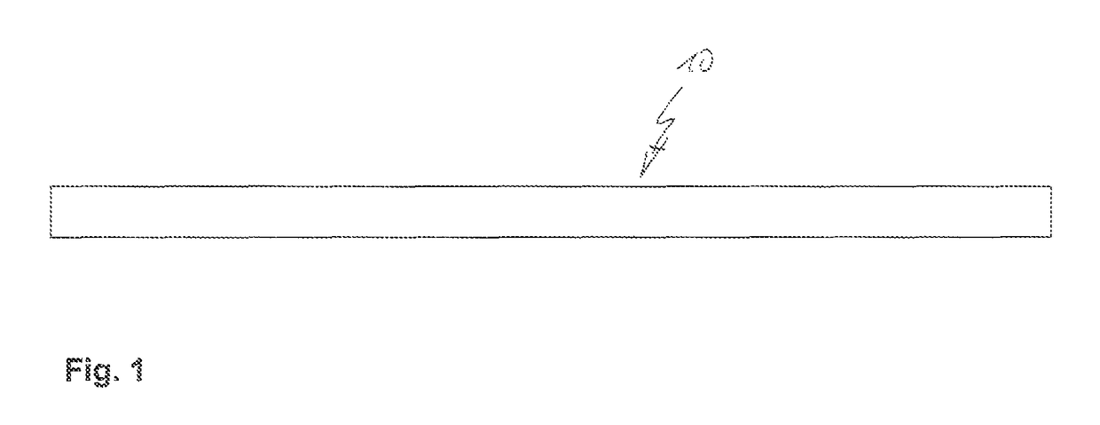
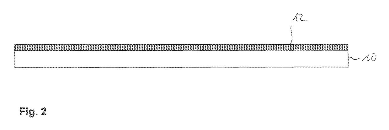
[0026]FIG. 1 shows a starting or base substrate 10 for an electronic sub-assembly according to the invention. The starting substrate 10 is made of an electrically conductive material. This can be copper sheet metal. Alternatively, it can also be a substrate made of a material with a low heat expansion coefficient; e.g., of a suitable iron-nickel alloy covered with copper on both sides. An example for the latter is copper-Invar®-copper sheet metal (CIC sheet metal), as it is commercially available ready-made. Typical thicknesses of such a commercially available ready-made CIC layer are 150 μm of Invar® and 18 μm each of copper.

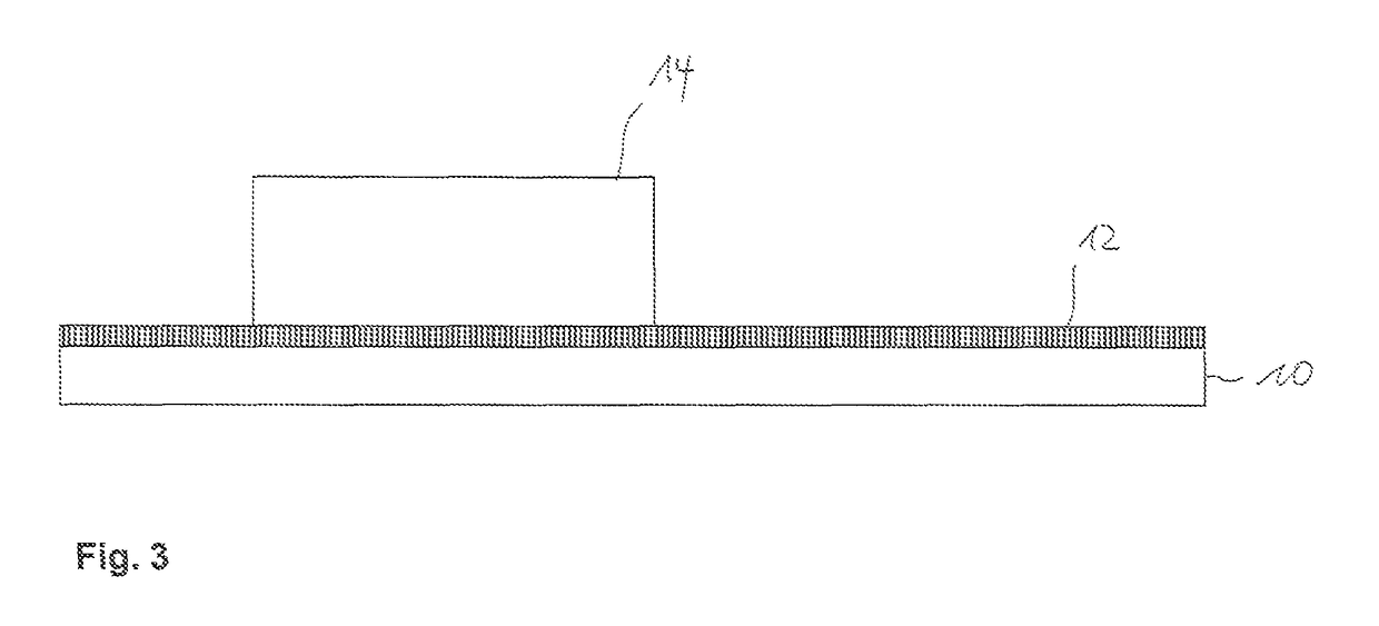
[0027]In a next step, a first layer 12 made of an electrically insulating material is deposited on the base or starting substrate 10 (cf. FIG. 2). Said first layer is a layer made of a material that contains resin and is curable, as it is well known in the production of electronic sub-assemblies. The person skilled in the art also calls such a material a prepre...


PUM


Abstract

An electronic sub-assembly (36) comprising at least one electronic component (14) embedded in a sequence of layers, wherein the electronic component (14) is arranged in a recess of an electrically conductive central layer (16) and directly adjoins a resin layer (12, 20) on each side.

Description

TECHNICAL AREA[0001]The present invention relates to an electronic sub-assembly as well as a method for producing an electronic sub-assembly.DESCRIPTION OF THE STATE OF THE ART[0002]Electronic sub-assemblies are known. They usually comprise a more or less complex layered structure made of (electrically) conductive and non-conductive layers, and are—within or on the sequence of layers—equipped with electronic components (such as power semiconductors, etc.). Connection of the components is made through the layers of the layered structure above them.SUMMARY OF THE INVENTION[0003]According to the invention, a method for producing an electronic sub-assembly with the features as disclosed herein, as well as an electronic sub-assembly with the features as disclosed herein, and a printed circuit board (PCB) as disclosed herein comprising an electronic sub-assembly according to the invention are provided.[0004]The idea according to the invention consists in providing an electronic sub-assemb...

Claims


Application Information

Patent Timeline
Patent Type & Authority Patents(United States)
IPC IPC(8): H05K3/46H05K1/18H05K3/30H01L25/00H01L23/00H01L23/498H01L23/538H01L25/07H01L21/48
CPCH01L25/072H01L21/486H01L21/4857H01L23/49822H01L23/49827H01L23/49844H01L23/5389H01L24/19H01L24/20H01L24/24H01L24/25H01L24/82H01L24/83H01L25/50H05K1/185H05K3/4608H05K3/30H05K1/188H01L2924/3511H01L2924/13091H01L2224/92144H01L24/29H01L24/32H01L24/75H01L24/92H01L2224/04105H01L2224/221H01L2224/24137H01L2224/2518H01L2224/32013H01L2224/75252H01L2224/7625H01L2224/82001H01L2224/82007H01L2224/82039H01L2224/82105H01L2224/832H01L2224/83048H01L2224/8388H01L2224/83192H01L2924/00012H01L2224/274H01L2924/00014H01L2224/2929H01L2224/06181
Inventor GOTTWALD, THOMASNEUMANN, ALEXANDER
Owner SCHWEIZER ELECTRONIC
Why Eureka
Try Eureka