System and method of optically inspecting surface structures on an object

a surface structure and optical inspection technology, applied in the field of optical inspection of surface structures on objects, can solve the problems of difficult, if not impossible, to reverse the fabrication steps in any cost-effective way, and each fabrication step is expensive,

Inactive Publication Date: 2001-09-18
SEMICON TECH & INSTR +1
View PDF5 Cites 50 Cited by
  • Summary
  • Abstract
  • Description
  • Claims
  • Application Information

AI Technical Summary

Problems solved by technology

Each fabrication step is expensive and adds significantly to the cost of the semiconductor wafer.
Furthermore, fabrication steps such as etching and ion implantation are difficult, if not impossible, to reverse in any cost-effective way.
Photoresist defects are those anomalies that will result in impaired or altered electrical characteristics when fabrication of the die is complete, causing it to be rejected.
Common photoresist defects include alignment errors, missing photoresist structures, contamination, and skewed photoresist.
Other available methods include electronic, ion beam, and X-ray imaging, but they are slower and more expensive than optical inspection because these imaging techniques illuminate and reconstruct only one point at a time.
Laser imaging techniques that capture and compare the angle of reflection of laser beams can also be employed, but they lack comparable precision in reporting the position of defects.
Although numerous advances have been recently achieved in the optical detection, analysis, and classification of defects, present systems still have disadvantages associated with efficiency, accuracy, and adaptability in manufacturing.

Method used


Image

  • System and method of optically inspecting surface structures on an object
  • System and method of optically inspecting surface structures on an object
  • System and method of optically inspecting surface structures on an object

Examples


Embodiment Construction

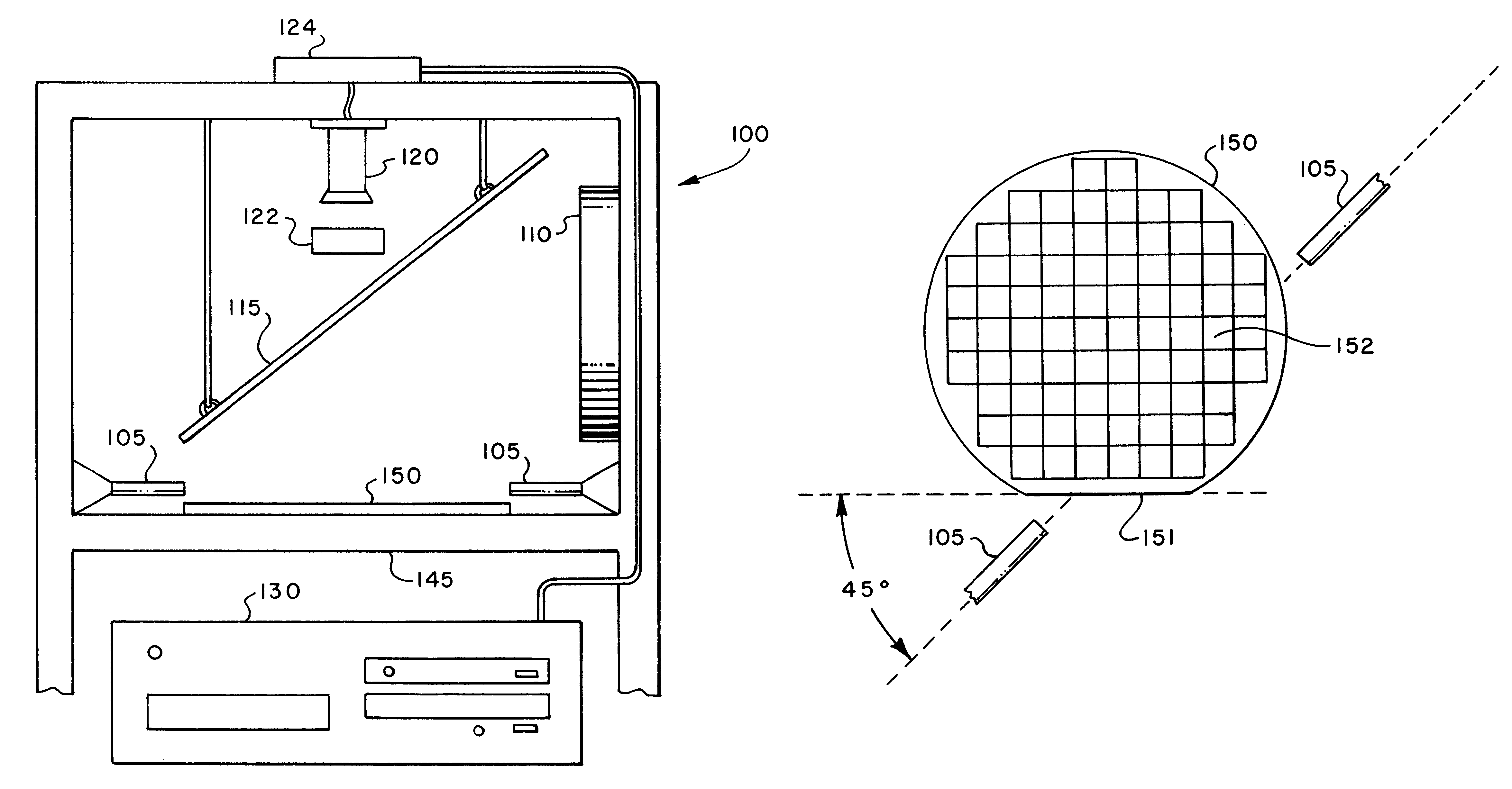
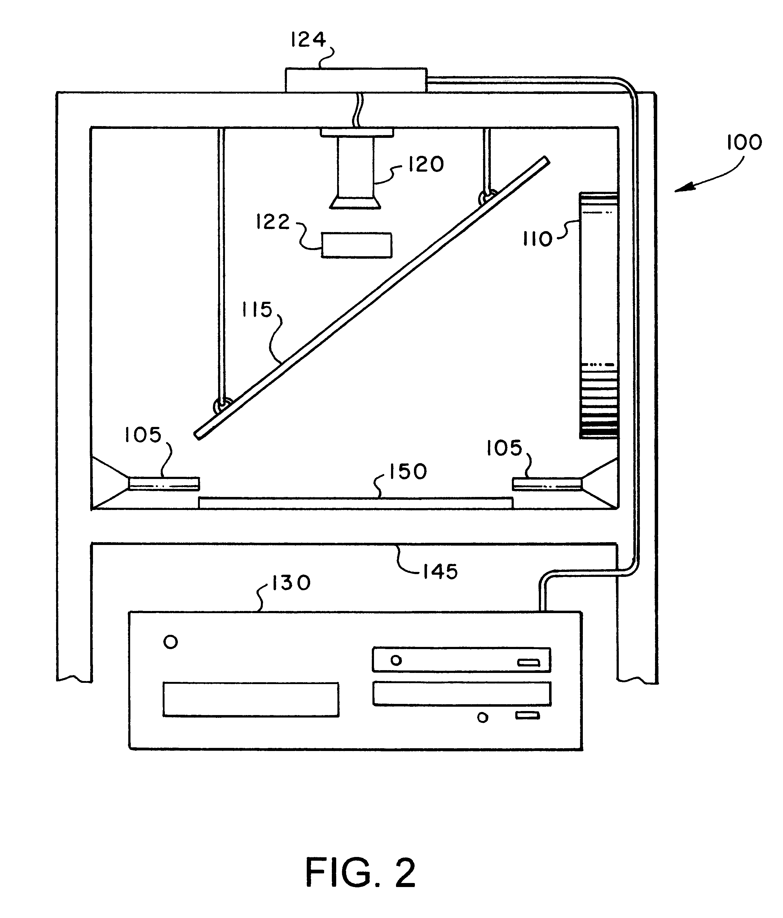
The present invention provides a system and method of optically inspecting the surface of an object. The preferred embodiment is described as a system and method of optically inspecting photoresist structures on the surface of semiconductor wafer dice. By using a unique configuration of object illumination sources, the present invention achieves the result of defect detection more efficiently and accurately than can be obtained using conventional methods and systems.

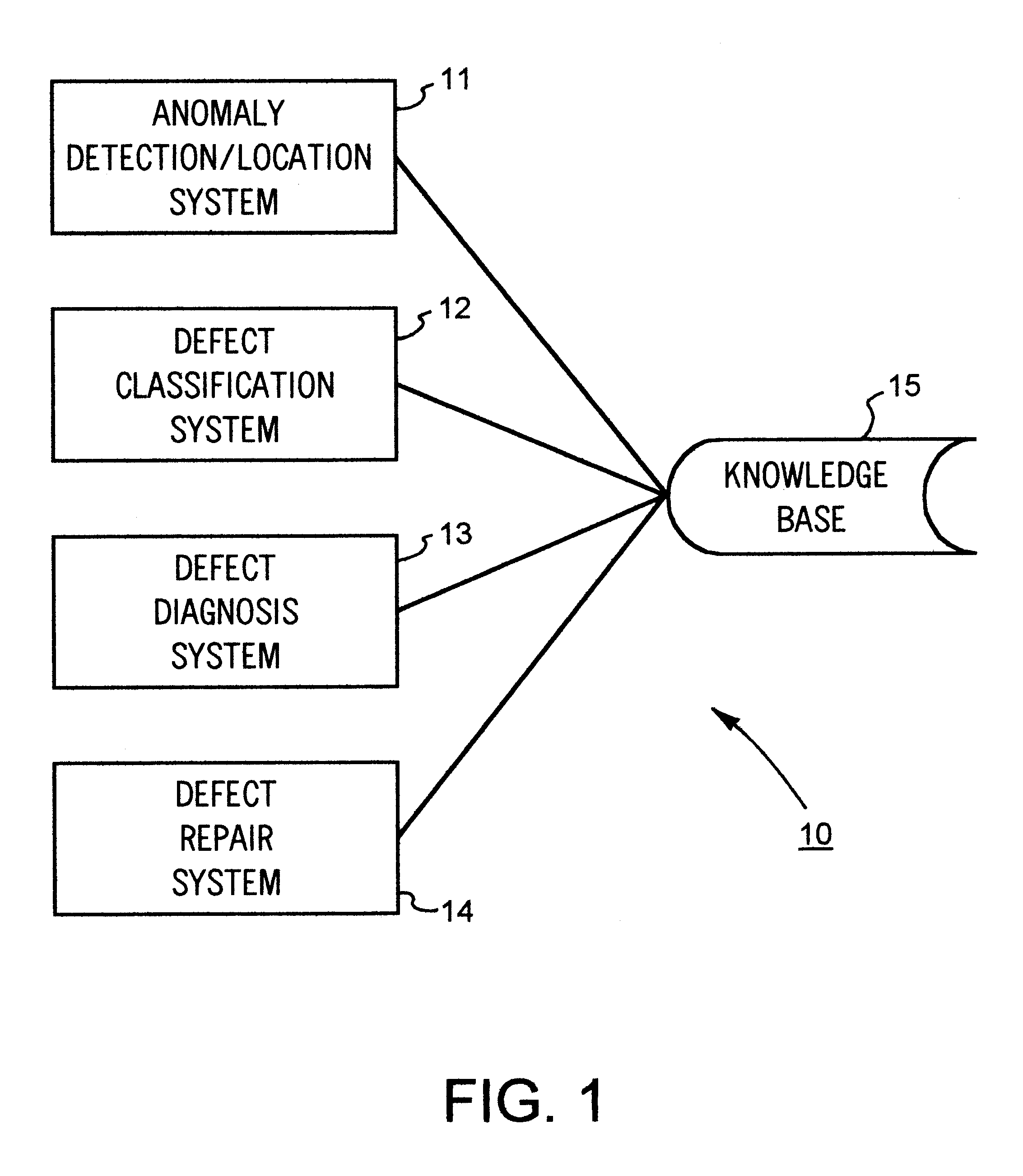
In a preferred embodiment, the present invention is used in an optical Integrated Defect Detection, Classification, Diagnosis, and Repair (IDDCDR) system. FIG. 1 is a functional block diagram showing the basic components of a typical IDDCDR system 10. An anomaly detecting and locating inspection system 11 includes the actual components by which a manufactured object is positioned in a suitable environment, properly illuminated, and an image of the energy reflected off of the object is captured. Using this image, a defect...


PUM

PropertyMeasurementUnit
azimuth angleaaaaaaaaaa
angleaaaaaaaaaa
heightaaaaaaaaaa

Abstract

A system and method of optically inspecting structures on the surface of an object, such as a semiconductor wafer. A platform is used to support the object under examination, and provided thereat are lights or other energy sources for illumination disposed at a selected angular orientation. Optimum illumination is achieved by orienting two opposing lateral energy sources to direct energy along the surface of the object at a very low angle, and using them in conjunction with a coaxial light source that emits energy, which is directed downward toward the surface. Energy reflected back from the surface is captured as an image by a suitable device such as a CCD camera. The lighting may be controlled by an attached computer, which can also be used to process and store the captured image and analyze it to detect and catagorize defects in the object being inspected.

Description

1. Technical Field of the InventionThe present invention relates to the inspection of surface structures on an object and, more specifically, to a system and method for optically inspecting the surface of an object having surface structures thereon.2. Description of Related ArtOptical inspection of an article of manufacture encompasses a variety of techniques that make use of the patterns produced by energy reflecting off (or passing through) the object being inspected. These reflections constitute an image that can be examined, compared with other images, stored, and otherwise analyzed. Examination may be performed by the human eye, with or without the aid of a magnifying device, such as a microscope. Or the image may be `captured` by a camera and converted directly into electronic data for storage and analysis, either immediately or at some time in the future. In the manufacturing process, optical inspection can be done for the purpose of final acceptance or rejection, or as an in...

Claims


Application Information

Patent Timeline
Patent Type & Authority Patents(United States)
IPC IPC(8): G01N21/95G01N21/88
CPCG01N21/9503G01N21/9501
Inventor LIN, YOULINGHARRIS, CHARLESGUEST, MAXEPP, GEORGE C.
Owner SEMICON TECH & INSTR
Why Eureka
Try Eureka