

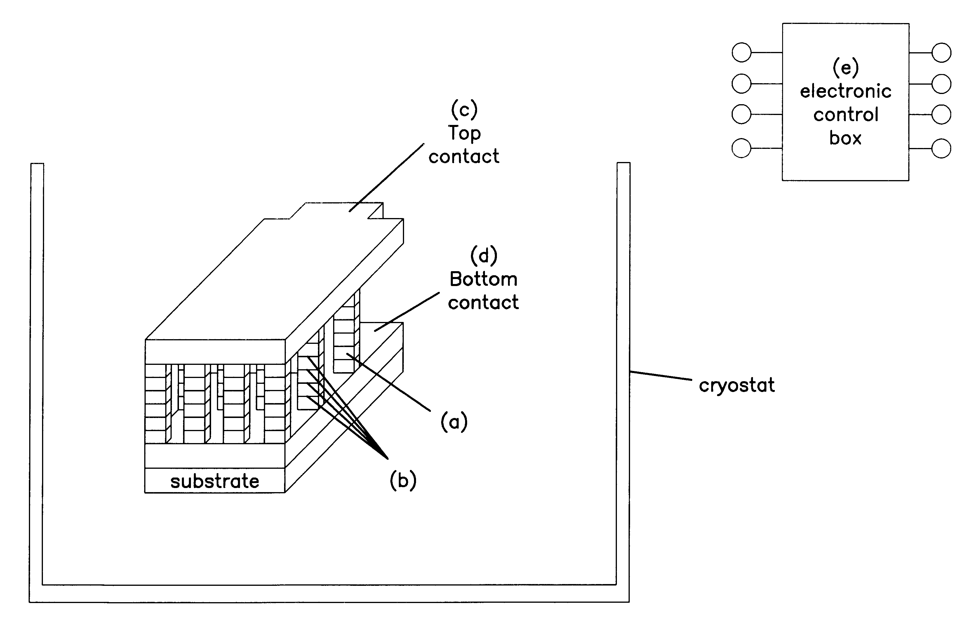
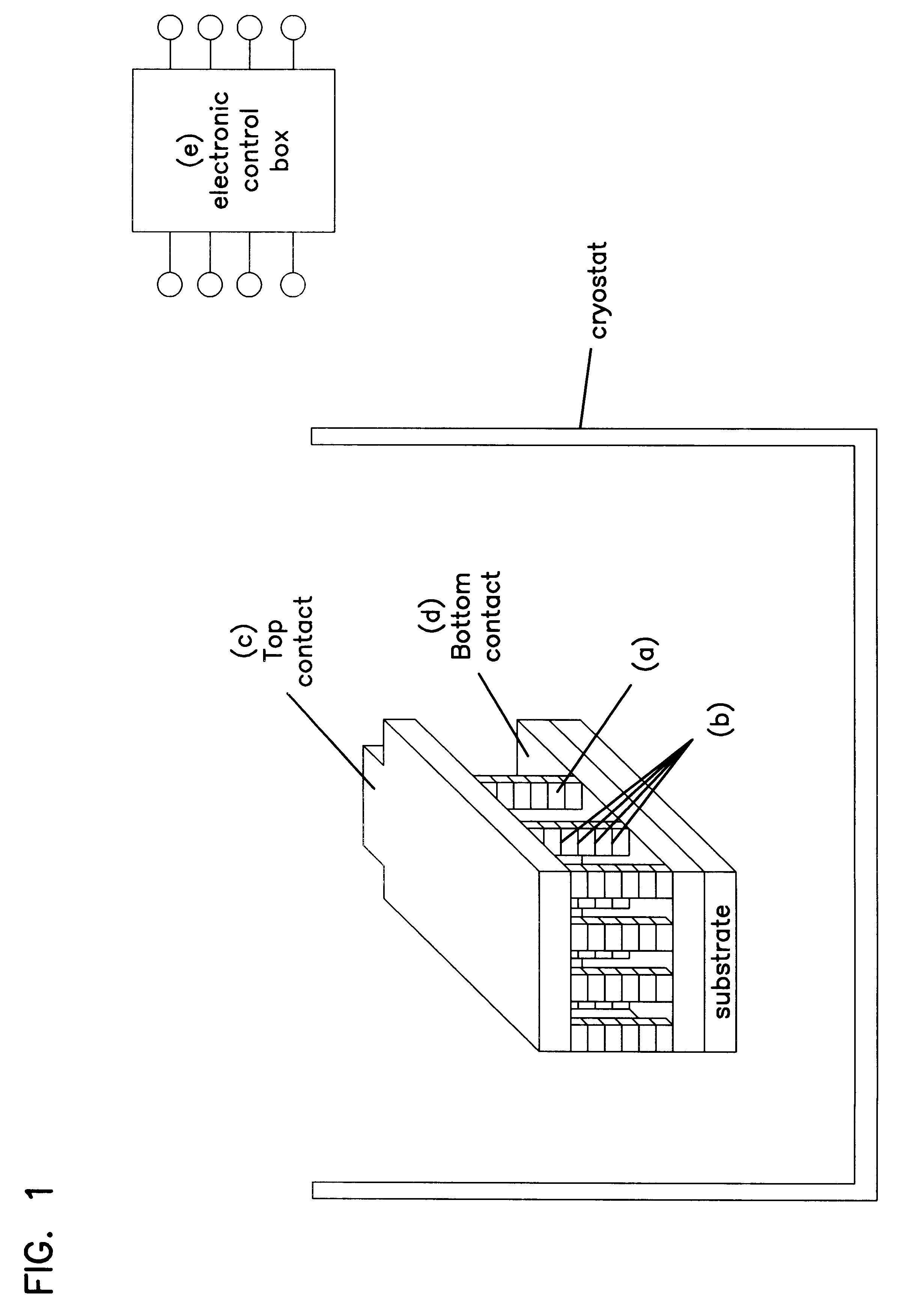
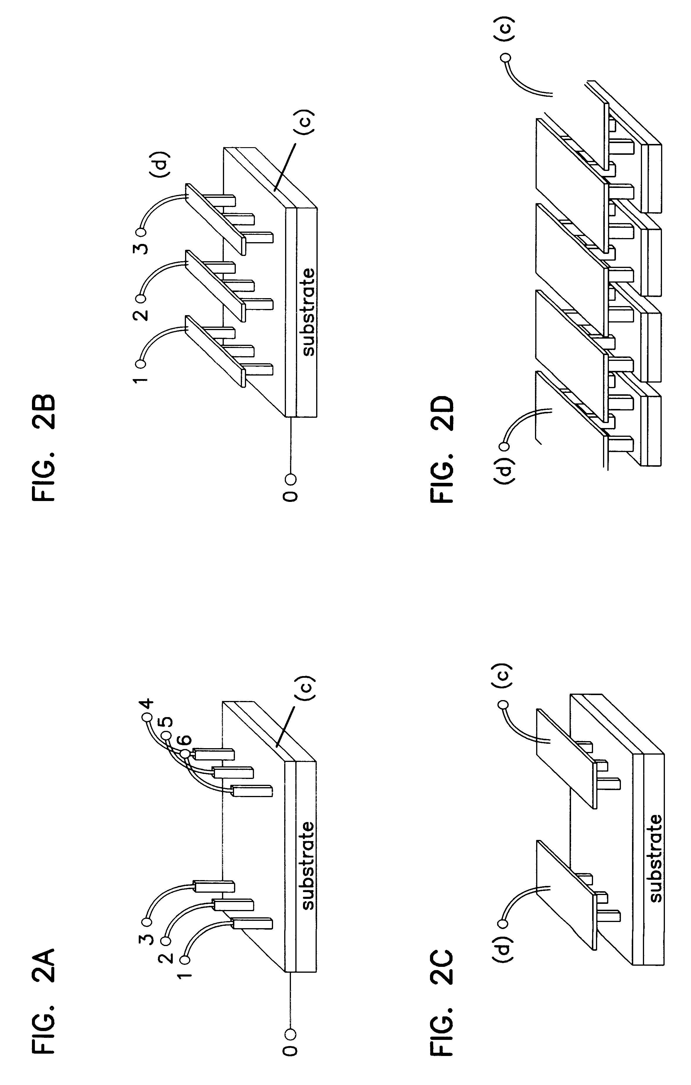
Josephson junction array device, and manufacture thereof
a junction array and junction technology, applied in the direction of superconducting magnets/coils, magnetic bodies, magnetic device details, etc., can solve the problems of no such application realized (i.e., reduced to practice), no phase locking, no phase locking, etc., and no intention of controlling radiation emission frequency
- Summary
- Abstract
- Description
- Claims
- Application Information
AI Technical Summary
Benefits of technology
Problems solved by technology
Method used
Image

Examples
second embodiment
(x) the Tunneltron using bulk single crystals of highs-T.sub.c superconductor materials.
Indeed, as it will be obvious to one of average skill in the art that the processes and apparatus described in sections (ii)-(ix) above, can be also produced by fully analogous steps involving high-quality single crystals of high-T.sub.c superconductors. The same photolithographic techniques and steps, including etching and ion-milling, as well as subsequent overgrowths by another high-T.sub.c superconductor layer (HTS-2) for the top conducting electrode, can also be employed in this case. The main limiting factor here is the uniformity of the Josephson junctions in one mesa and between different mesas. Another is the limited flexibility in controlling the materials parameters such as j.sub.c or R. But within these constraints, the same ideas embodied in the present invention of the Tunneltron can also be practiced here, thus constituting just another special embodiment of the same invention.
third embodiment
(Xi) the Tunneltron using conventional (low-temperature) superconducting materials.
Further fully analogous embodiments of the present apparatus of invention can be realized by using conventional (low-temperature) superconducting materials, for example Nb / A10 .sub.x Nb or NbCN / MgO / NbCN tunnel junctions. As it will be obvious to one of average skill of the art, one can use completely analogous thin-film growth techniques and photolithographic steps to produce the apparatus of this invention also with these superconducting materials. There will be in this case some additional constraints coming from less favorable materials parameters.
First, because of the lower critical temperatures (T.sub.c =9.2 K in Nb and T.sub.c =16 K in NbN or NbCN, etc.) the gap frequencies in these materials are also substantially lower (.nu..sub.g =0.9 THz in Nb, and .nu..sub.g =1.7 THz in NbN) compared to those in high-T.sub.c superconductor materials (up to .nu..sub.g =5-10 THz). Hence, with low-temperature ...
PUM
 Abstract
Description
Claims
Application Information