Projection having a micro-aperture, probe or multi-probe having such a projection and surface scanner, aligner or information processor comprising such a probe

a technology of projection and aperture, which is applied in the direction of material analysis using wave/particle radiation, instruments, nuclear engineering, etc., can solve the problems of difficult to realize a process that can produce a number of micro-apertures in an integrated manner, the difficulty of precisely controlling the diameter of the micro-aperture and the inability to produce a number of micro-apertures in any of the known techniques

Inactive Publication Date: 2002-04-23
CANON KK
View PDF8 Cites 27 Cited by
  • Summary
  • Abstract
  • Description
  • Claims
  • Application Information

AI Technical Summary

Problems solved by technology

Also, the process of forming a micro-aperture in any of the known techniques will inevitably show a poor productivity and it is difficult to realize a process that can produce a number of micro-apertures in an integrated manner.
Additionally, the known techniques are accompanied by the difficulty of precisely controlling the diameter of the micro-aperture to ensure a reliable degree of reproducibility.

Method used


Image

  • Projection having a micro-aperture, probe or multi-probe having such a projection and surface scanner, aligner or information processor comprising such a probe
  • Projection having a micro-aperture, probe or multi-probe having such a projection and surface scanner, aligner or information processor comprising such a probe
  • Projection having a micro-aperture, probe or multi-probe having such a projection and surface scanner, aligner or information processor comprising such a probe

Examples


example 1

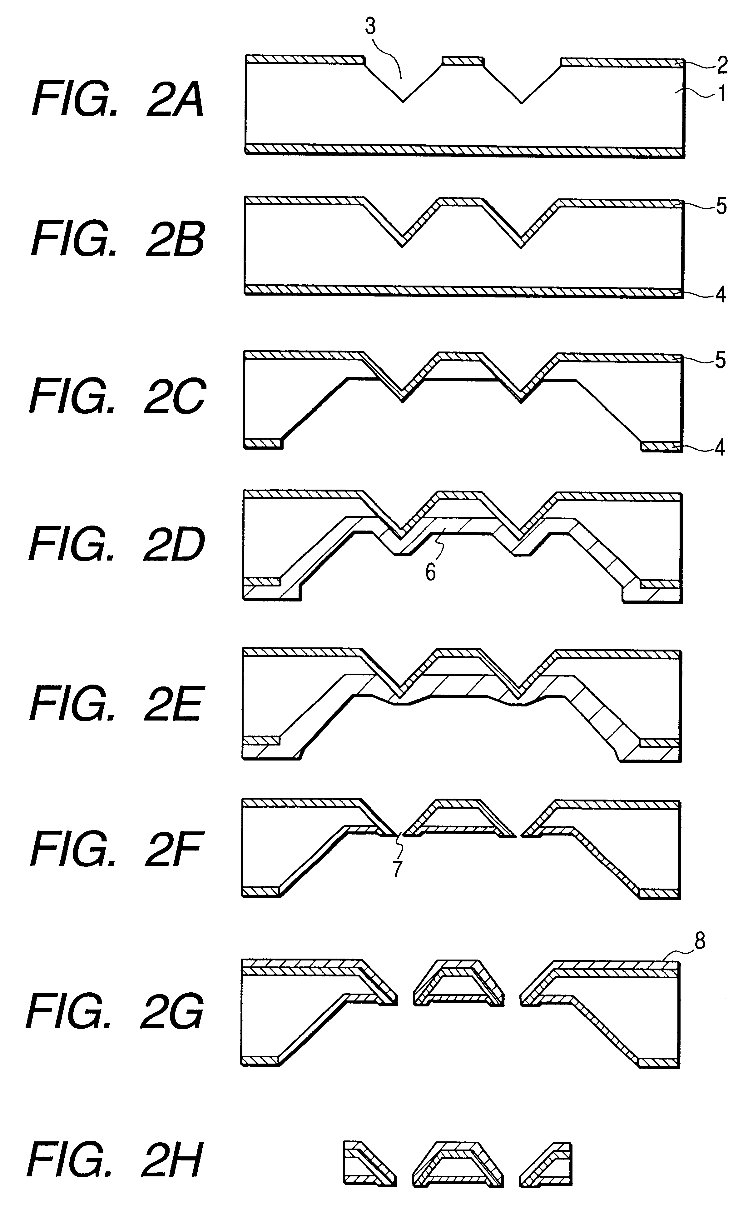
relates to an array of 100 micro-apertures arranged in the form of a 10.times.10 matrix on a silicon substrate (see FIG. 3A) and a method of forming the array. An array of micro-apertures as prepared in Example 1 may typically be used to expose a sheet of photoresist to light to produce a micro-pattern by irradiating light from the side opposite to the side where the micro-apertures are arranged, while holding the photoresist so close to the micro-apertures as to make it exposed to evanescent light coming from the micro-apertures.

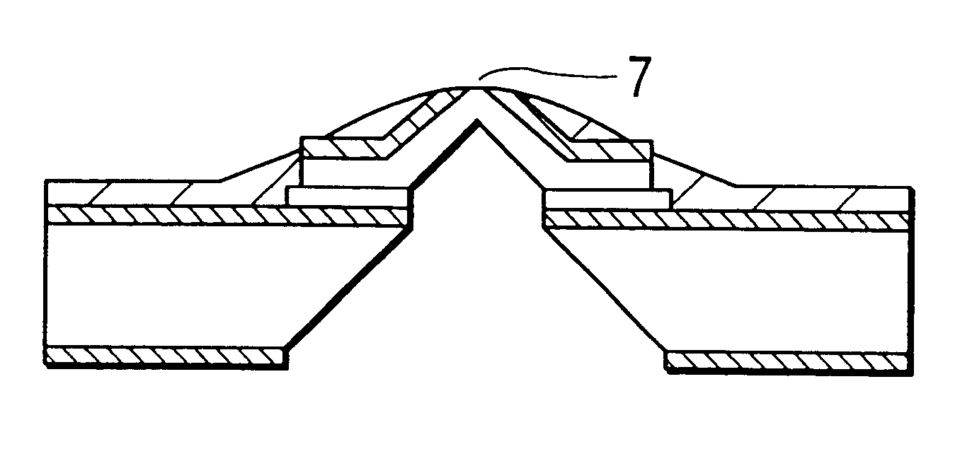
FIGS. 2A through 2H are schematic cross sectional views of an array of micro-apertures prepared in Example 1, showing different preparation steps as is will be described hereinafter.

A thermally oxidized silicon oxide film was formed to a thickness of 100 nm as protective layer 2 on a single crystal silicon wafer substrate 1 having a crystal plane of (100). Then, the protective layer 2 was patterned to expose the silicon by 50 .mu.m square by photolithograph...

example 2

This example relates to an optical probe formed on a substrate comprising a projection having a micro-aperture at the tip thereof.

A probe as prepared in Example 2 may typically be used to change the state of the surface of a micro-area of photoresist 20 by introducing light from the back side of the probe and irradiating the micro-area with evanescent light through the micro-aperture of the probe (see FIG. 5A).

It may also be combined with a light receiving device 22 and used in a microscope for detecting light in a near field (see FIG. 5B).

FIGS. 4A through 4F are schematic cross sectional views of an optical probe having a micro-aperture prepared in Example 2, showing different preparation steps. Now, the process of forming an optical probe having a micro-aperture will be described by referring to FIGS. 4A through 4F.

A thermally oxidized silicon oxide film was formed to a thickness of 100 nm as protective layer on a single crystal silicon wafer first substrate 11 having a crystal pl...

example 3

Example 3 relates to an optical multi-probe having an array of 100 optical probes, each having a projection and a micro-aperture at the top of the projection, arranged in the form of a 10.times.10 matrix on a substrate (see FIG. 7).

Each of the optical probes is provided with a light emitting device that is a surface emitting laser and wiring electrodes for driving it. An optical multi-probe as prepared in Example 3 may typically be used to change the state of the surface of a micro-area of photoresist by irradiating it with near-field light from each of the probes.

The rate of forming micro-patterns can be improved by intra-planarly scanning photoresist, turning on and off each of the probes in a controlled manner. While each probe having a micro-aperture is combined with a light emitting device in the example, the multi-probe may be combined with light receiving devices such as avalanche photodiodes to produce a multi-light-receiving device unit.

FIGS. 6A through 6E are schematic cro...


PUM

PropertyMeasurementUnit
temperatureaaaaaaaaaa
thicknessaaaaaaaaaa
depthaaaaaaaaaa

Abstract

A projection having a micro-aperture on the tip is formed. Firstly, a projection or a dent is formed on a substrate. Then, a film is formed on the surface of the projection or of the opposite side of the dent so as to make the film thin at and near the tip of the projection or the dent. The film is subsequently etched to expose the tip, which is further etched to produce a micro-aperture. Preferably, the film is formed of a thermo-plastic material such as glass, especially phospho-silicate glass to produce a viscous flow under heated conditions. The probe having a micro-aperture can be used for a surface scanner, an aligner or an information processor.

Description

1. Field of the InventionThis invention relates to a method of forming a micro-aperture. It also relates to a projection having such a micro-aperture, to a probe or multi-probe having such a projection or projections and also to a surface scanner (surface-observing system), an aligner (exposure system) or an information processor comprising such a probe. More particularly, the present invention relates to a method of manufacturing a micro-tip for detecting or irradiating evanescent light to be used for a near-field optical microscope and to a probe having such a micro-tip.2. Related Background ArtThe invention of the scanning tunneling microscope (hereinafter referred to as STM) made it possible to visually observe the electron structure of surface atoms of an electric conductor [G. Binnig et al., Phys. Rev. Lett. 49, 57 (1982)] and hence a real space image of a specimen to be dimensionally measured with an enhanced degree of resolution regardless if the specimen is monocrystalline ...

Claims


Application Information

Patent Timeline
Patent Type & Authority Patents(United States)
IPC IPC(8): G12B21/06G12B21/00H01J37/09G01B11/30C23F4/00G01B21/30G01N37/00G01Q60/22G01Q70/06G01Q70/10G01Q80/00G11B9/00G11B9/14H01J37/28H01L21/027
CPCB82Y20/00G01Q60/22H01J37/09B82Y35/00
Inventor SHIMADA, YASUHIROYAMAZAKI, TAKEO
Owner CANON KK
Why Eureka
Try Eureka