Stacked printed circuit board memory module and method of augmenting memory therein

a printed circuit board memory module and memory module technology, applied in the direction of manufacturing tools, fixed connections, coupling device connections, etc., can solve the problems of limiting the amount of pcb real estate available for additional memory ics, pcbs generally cannot be increased in length or height, and traditional memory packaging schemes have become inadequa

Inactive Publication Date: 2002-07-09
MICRON TECH INC
View PDF23 Cites 99 Cited by
  • Summary
  • Abstract
  • Description
  • Claims
  • Application Information

AI Technical Summary

Problems solved by technology

However, as computer system speeds and memory requirements have continued to increase and more integrated devices are incorporated onto PCBs, traditional memory packaging schemes have become inadequate.
However, the PCBs generally cannot be increased in length or height due to space limitations imposed by available areas on motherboards and within computer housings thereby limiting the amount of PCB real estate available for additional memory ICs.
However, increasing the number of chips on individual boards consequently increases the length of the traces between chips and other PCBs.
Other transmission line problems occur when these high speed signals are transmitted over traces that are too long.
Such problems include reflections, cross-talk, and electromagnetic induction.
However, decreasing die size while increasing memory density leads to greater costs.
There have been increases to a 128 Megabit and 256 Megabit die but with a corresponding increase in cost of approximately five to six times.
While this solution increases the memory density, heat dissipation becomes a problem.
Each of the individual ICs become hot and the heat cannot be properly dissipated from the PCB.
The increased heat causes the performance of the memory module to decrease and often fail.
As a result, the memory modules cannot be run at full performance.
Moreover, heat generation problems limit the number of memory modules that can be populated on a PCB, degenerating performance.
Therefore, the number of memory ICs that can be placed on any given PCB memory module is limited due to heat dissipation and other considerations.

Method used


Image

  • Stacked printed circuit board memory module and method of augmenting memory therein
  • Stacked printed circuit board memory module and method of augmenting memory therein
  • Stacked printed circuit board memory module and method of augmenting memory therein

Examples


Embodiment Construction

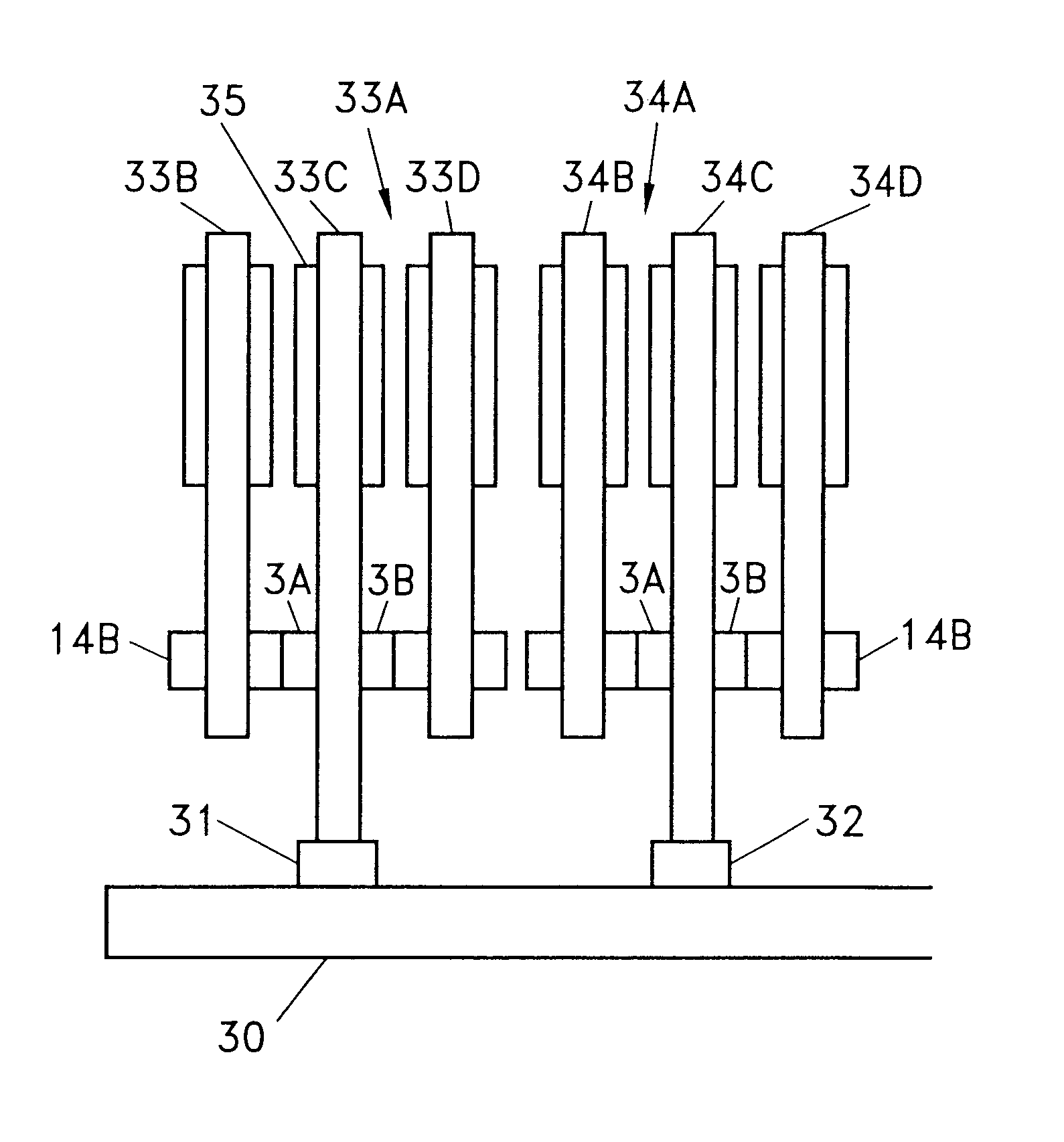
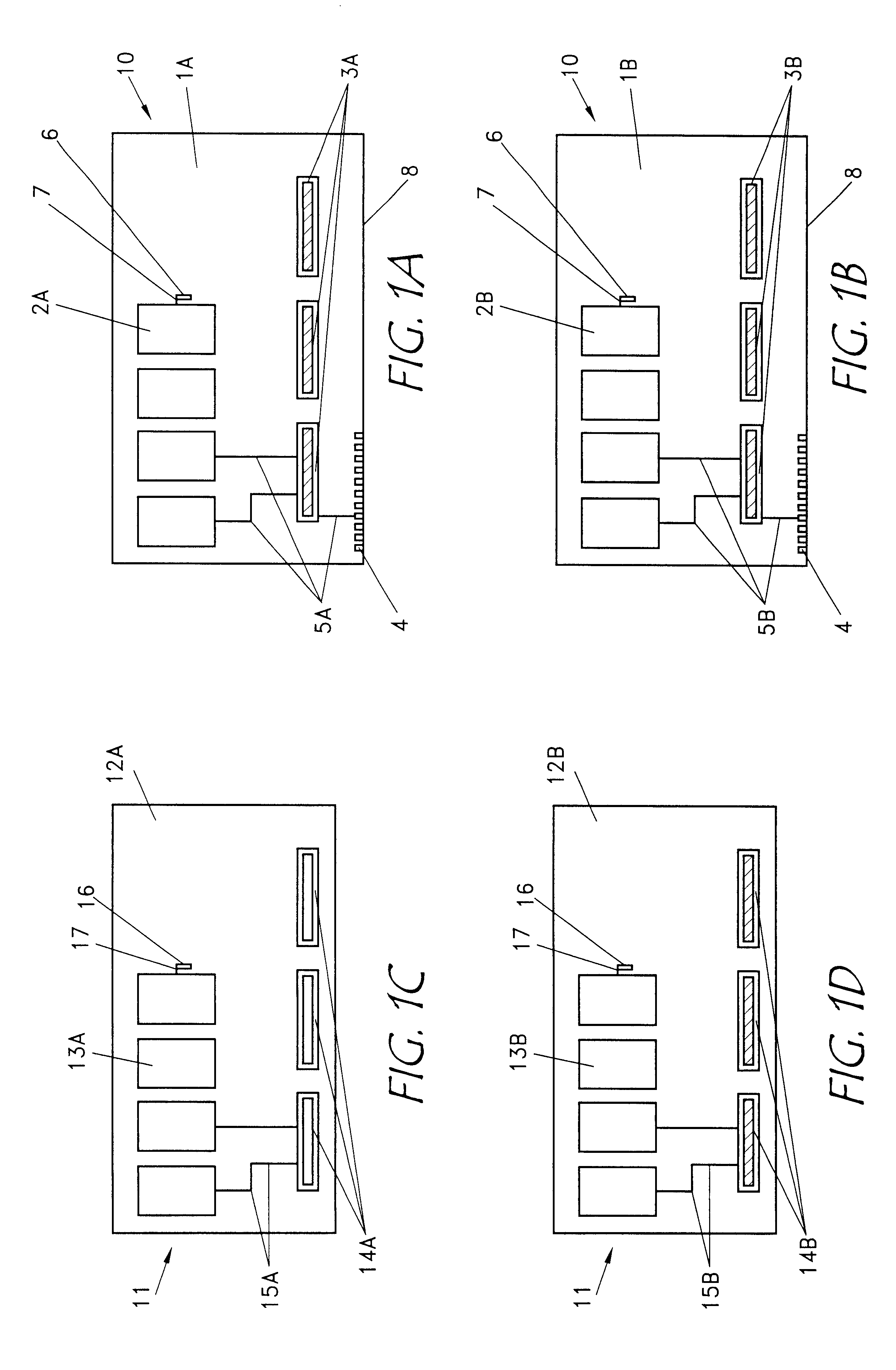
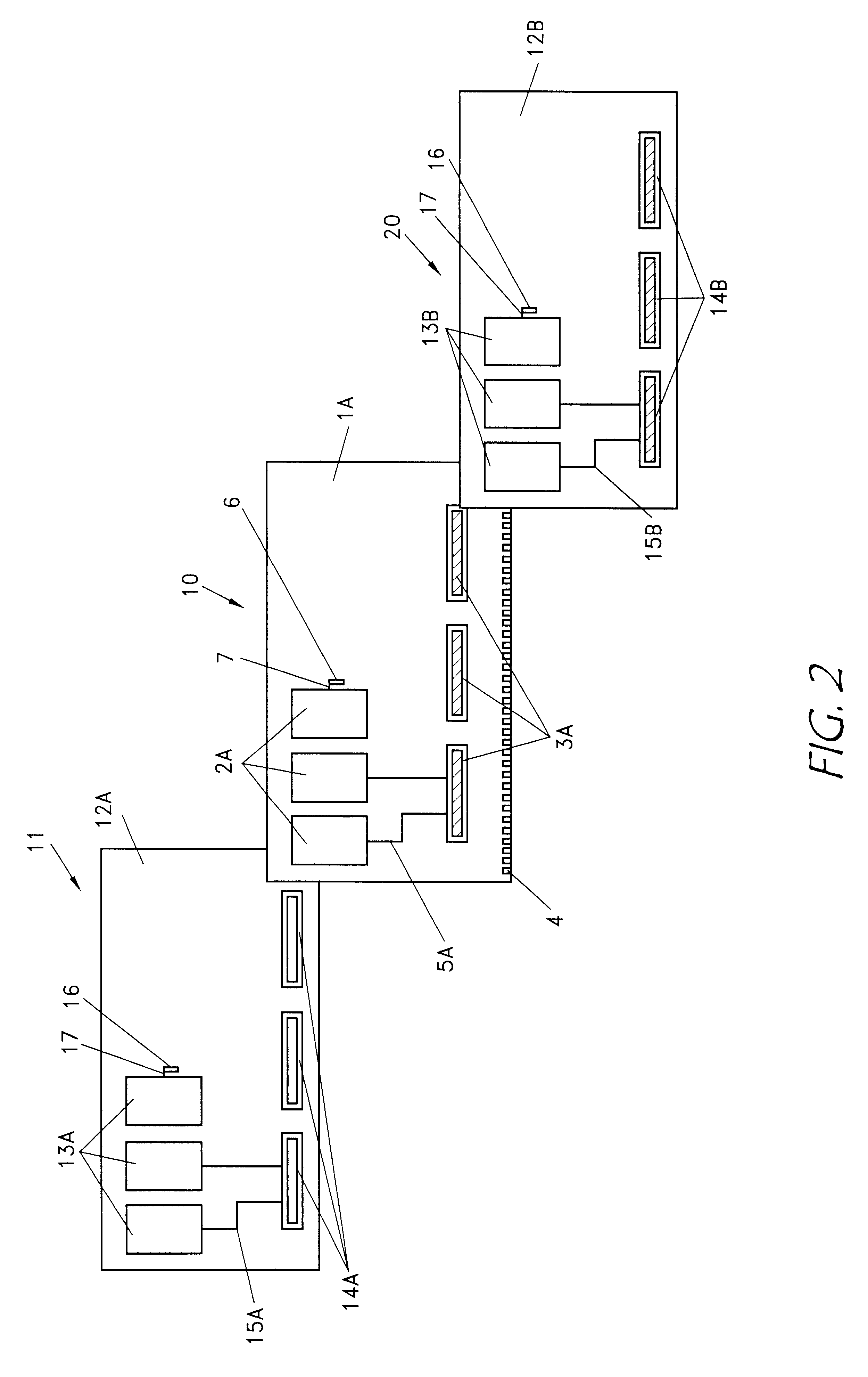
Referring to FIG. 1A, there is shown a front view of a primary circuit board 10 with the first surface 1a facing forward. Electronic components 2a are mounted on the first surface 1a. Only four individual electronic components 2a are shown in the figure for the purpose of clarity. Additional components may be added in other implementations of the invention. In an implementation of the invention electronic components 2a may be Synchronous Dynamic Random Access Memory (SDRAM) ICs. Vias 6 are present on the surface 1a of the primary circuit board 10 in order to provide access to couple the electronic components 2a on the first surface of the primary board 1a to the other side of the board. Only one via 6 is shown in the figure. Via conductors 7 provide the electric coupling to components on the other side of the board. Only via conductor 7 is shown in the figure. Primary connectors 3a are also mounted on first surface 1a. In an implementation of the invention, female-type primary conne...


PUM

PropertyMeasurementUnit
conductiveaaaaaaaaaa
electrically coupleaaaaaaaaaa
densityaaaaaaaaaa

Abstract

A stacked printed circuit board memory module in which a plurality of daughter circuit boards can be stacked onto a primary circuit board. The primary board and each of the plurality of daughter boards have electronic memory ICs mounted on the respective surfaces. The primary board and each of the daughter boards have mounted connectors so that the boards can be electronically and mechanically interconnected with another board.

Description

The invention relates to high density memory systems for high-speed computer and network systems, and more particularly to an improved high density memory module.DESCRIPTION OF THE RELATED ARTWith the introduction of network servers and work stations that can utilize memory in the gigabyte range and can operate at speeds of 100 Mhz or higher, fast and high density memory modules are needed to reach these memory capacities and speeds. Present day computer systems typically include hundreds of discrete components mounted on printed circuit boards (PCBs) interconnected with wiring on the board. The PCBs may also include sockets and connectors for receiving additional components, component modules and multichip modules, and connectors to other PCBs.Computer memory often consists of one or more memory modules which plug into connectors on main printed circuit boards in computers (motherboards). The PCB memory module connector sockets are interconnected by a common set of address, data an...

Claims


Application Information

Patent Timeline
Patent Type & Authority Patents(United States)
IPC IPC(8): H05K1/14H05K7/02
CPCH05K1/144H05K7/023H01R9/096H01R12/52
Inventor WEBER, RICKLARSEN, COREYHOWARTH, JAMES
Owner MICRON TECH INC
Why Eureka
Try Eureka