Method and apparatus for data sampling

a data sampling and data technology, applied in the field of data sampling circuits, can solve problems such as the logic circuit cannot sample input data properly

Inactive Publication Date: 2002-10-29
LAPIS SEMICON CO LTD
View PDF5 Cites 10 Cited by
  • Summary
  • Abstract
  • Description
  • Claims
  • Application Information

AI Technical Summary

Benefits of technology

Accordingly, an object of the present invention is to provide a data sampling circuit in which input data are sampled at appropriate timings to provide reliability of data sampling even if the input data are phase-shifted.
Another object of the present invention is to provide a method in which input data are sampled at appropriate timings to provide reliability of data sampling even if the input data are phase-shifted.
In another embodiment, an average phase signal representing the average of phase of plural source clocks, provided in the past, is generated. One from the average phase signal and currently generated sampling clock is selected to provide a sampling clock to be actually used for sampling process. Preferably, a previous sampling clock and currently generated sampling clock are compared to detect a phase difference between them; and the sampling operation is prohibited when the phase difference between the previous sampling clock and currently generated sampling clock is larger than a predetermined threshold value. According to this embodiment, it is not necessary to generate a sampling clock for each cycle of the input data. As a result, power consumption of the circuit can be reduced.

Problems solved by technology

According to the conventional logic LSI, if the input data is shifted in phase, the logic circuit could not sample the input data properly and mistakenly generates an unexpected output data.

Method used


Image

  • Method and apparatus for data sampling
  • Method and apparatus for data sampling
  • Method and apparatus for data sampling

Examples


first preferred embodiment

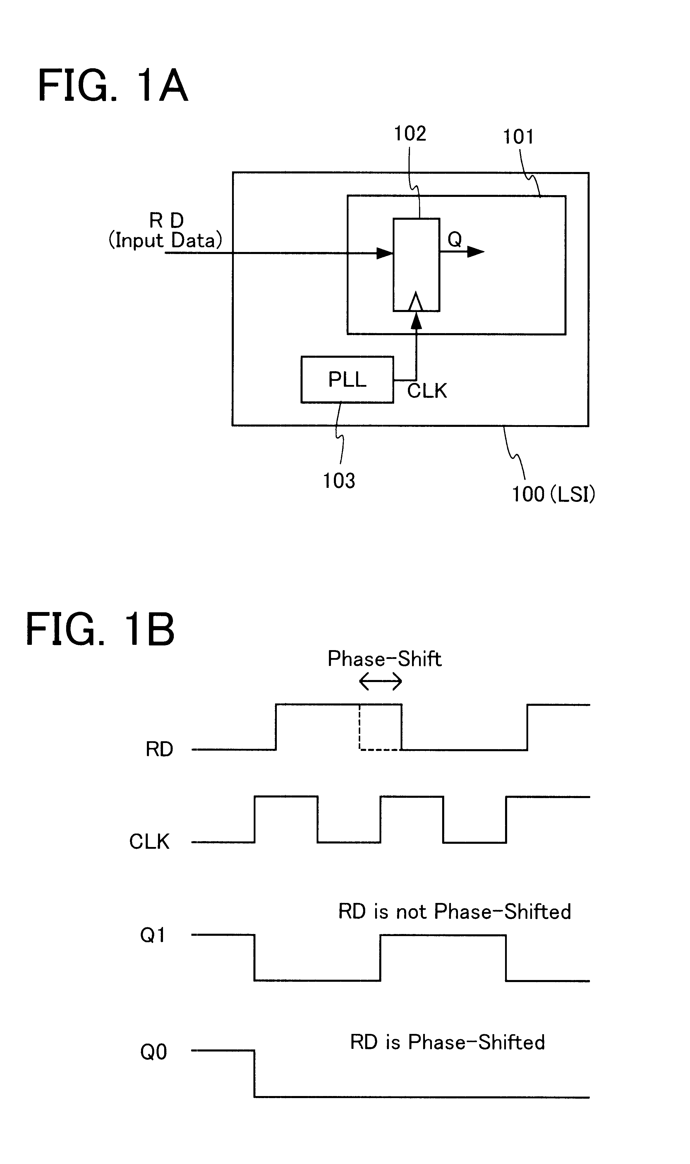
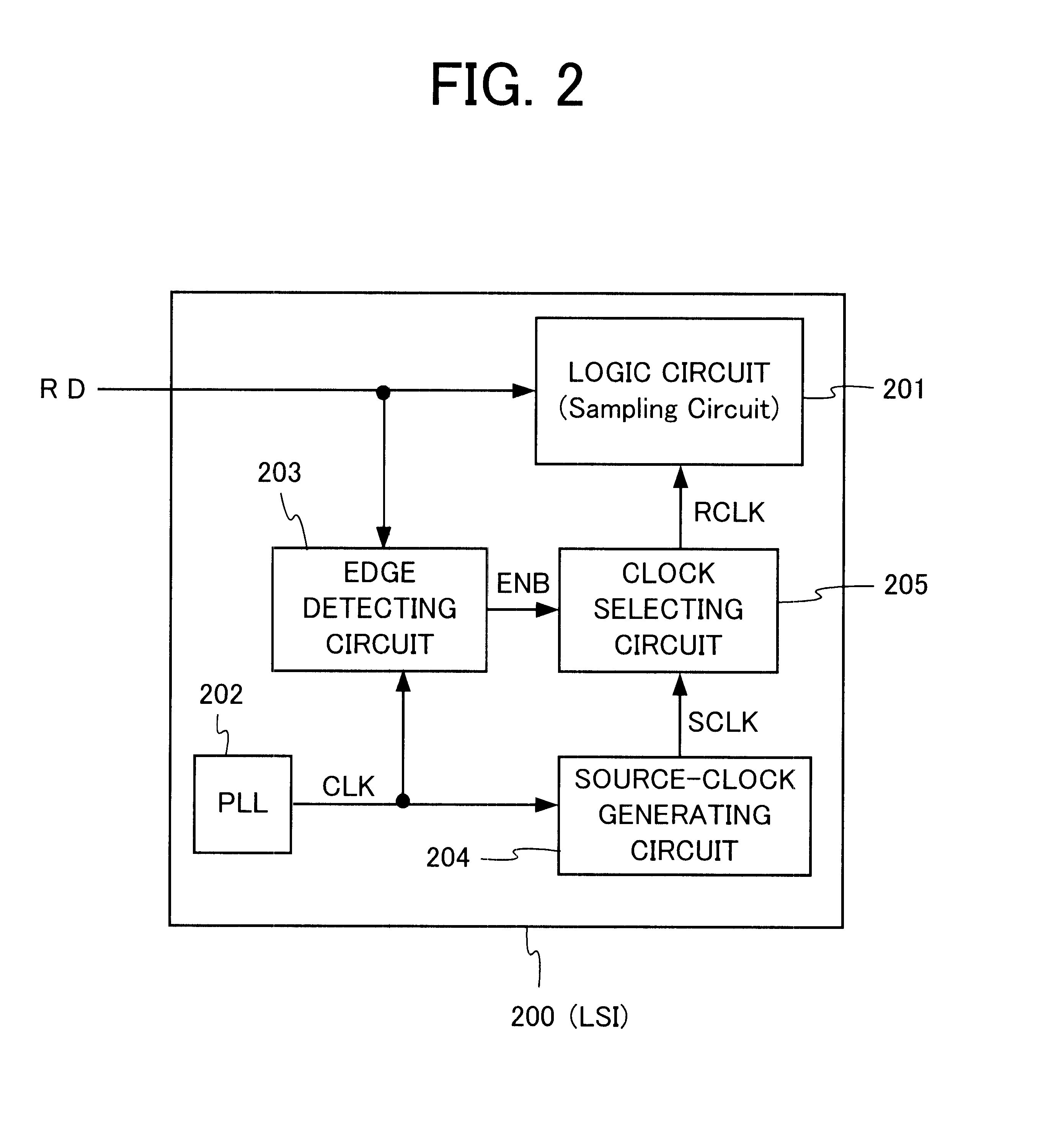
FIG. 2 is a block diagram showing a logic LSI according to a first preferred embodiment of the present invention. A logic LSI 200 according to the first preferred embodiment includes a logic circuit (sampling circuit) 201, a PLL circuit 202, an edge detecting circuit 203, a source-clock generating circuit 204 and a clock selecting circuit 205. Input data RD are supplied to the logic circuit 201 and edge detecting circuit 203. The PLL circuit 202 is connected at an output terminal to input terminals of the edge detecting circuit 203 and source-clock generating circuit 204. The PLL circuit 202 supplies a base clock CLK to the edge detecting circuit 203 and source clock generating circuit 204.

The edge detecting circuit 203 is connected to an output terminal to an input terminal of the clock-selecting circuit 205. The edge detecting circuit 203 supplies an ENB signal to the clock-selecting circuit 205. The edge detecting circuit 203 detects level-turning points of the input data RD in s...

second preferred embodiment

FIG. 6 is a block diagram showing a logic LSI according to a second preferred embodiment of the present invention. A logic LSI 300 according to the second preferred embodiment includes a logic circuit 301, a PLL circuit 302, an edge detecting circuit 303 and a sampling-clock generating circuit 304. Input data RD are supplied to the logic circuit 301 and edge detecting circuit 303. The PLL circuit 302 is connected at an output terminal to input terminals of the edge detecting circuit 303 and sampling-clock generating circuit 304. The PLL circuit 302 supplies a base clock CLK to the edge detecting circuit 303 and sampling-clock generating circuit 304.

The edge detecting circuit 303 is connected to an output terminal to an input terminal of the sampling-clock generating circuit 305 to supply an ENB signal thereto. The edge detecting circuit 303 detects level-turning points of the input data RD in synchronization with the base clock CLK and generates the ENB signal when a level-turning p...

third preferred embodiment

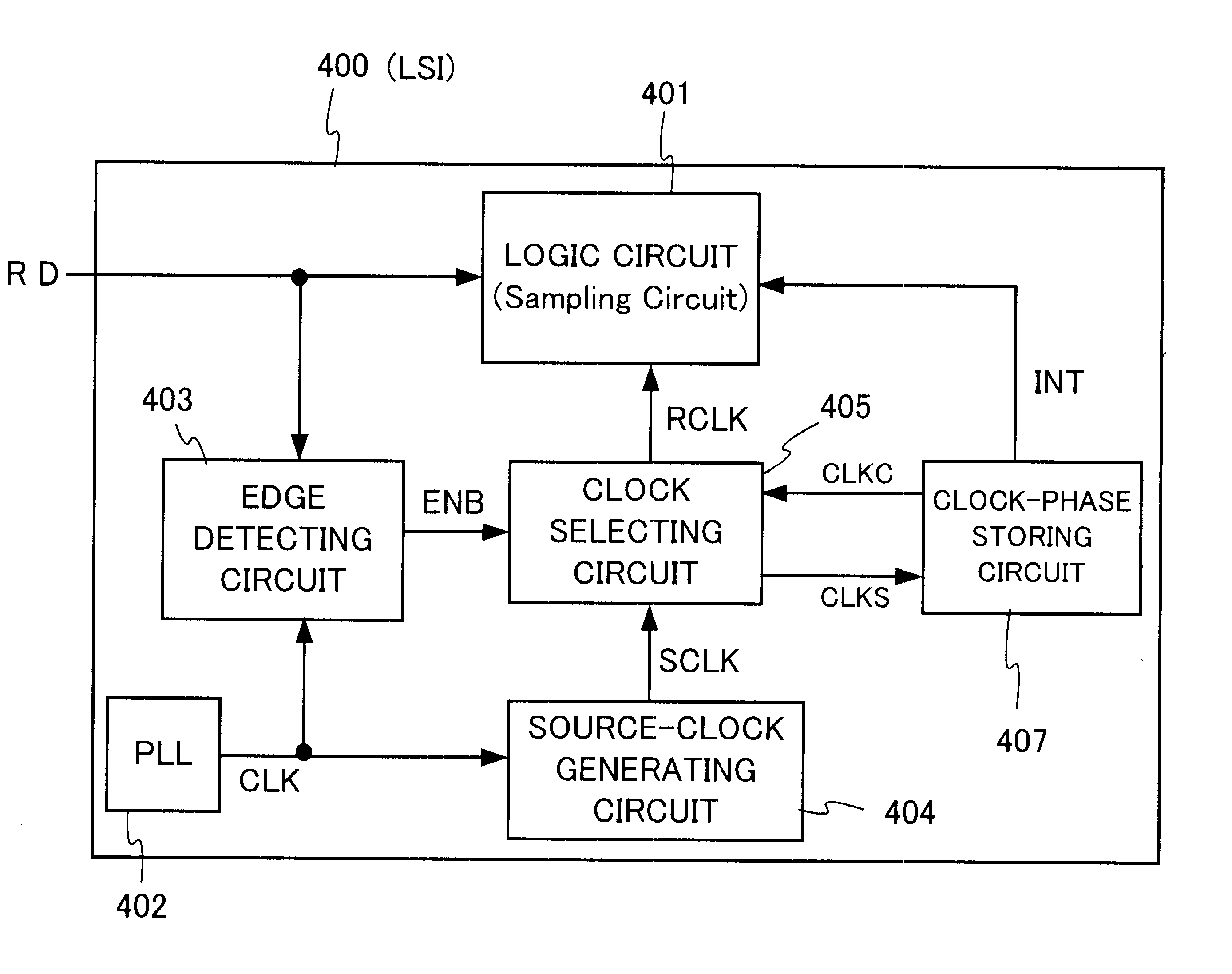
FIG. 10 is a block diagram showing a logic LSI according to a third preferred embodiment of the present invention. A logic LSI 400 according to the third preferred embodiment includes a logic circuit 401, a PLL circuit 402, an edge detecting circuit 403, a source-clock generating circuit 404, a clock selecting circuit 405 and a clock-phase storing circuit 407. Input data RD are supplied to the logic circuit 401 and edge detecting circuit 403. The PLL circuit 402 is connected at an output terminal to input terminals of the edge detecting circuit 403 and source-clock generating circuit 404 to supply a base clock CLK thereto.

The edge detecting circuit 403 is connected to an output terminal to an input terminal of the clock-selecting circuit 405 to supply an ENB signal thereto. The edge detecting circuit 403 detects level-turning points of the input data RD in synchronization with the base clock CLK and generates the ENB signal when a level-turning point of the input data RD is detected...


PUM


Abstract

A level-turning point of input data is detected; and a sampling clock is generated in response to the level-turning point of the input data. The input data are sampled in synchronization with the sampling clock.

Description

The present invention relates to a logic LSI in which input data are sampled in synchronization with a clock signal.A conventional logic LSI includes a logic circuit, a register and a PLL (Phase Locked Loop) circuit. The register is connected to a clock input terminal to an output terminal of the PLL circuit. The register receives input data and generates an output signal Q in synchronization with a clock signal generated in the PLL circuit to have a constant phase. In other words, the logic circuit samples the input data in synchronization with the constant clock signal.According to the conventional logic LSI, if the input data is shifted in phase, the logic circuit could not sample the input data properly and mistakenly generates an unexpected output data.OBJECTS OF THE INVENTIONAccordingly, an object of the present invention is to provide a data sampling circuit in which input data are sampled at appropriate timings to provide reliability of data sampling even if the input data a...

Claims


Application Information

Patent Timeline
Patent Type & Authority Patents(United States)
IPC IPC(8): H04L7/033
CPCH04L7/0338
Inventor NATSUME, KENICHI
Owner LAPIS SEMICON CO LTD
Why Eureka
Try Eureka