Stress-free socketed optical display package with die non-rigidly attached to containment structure

Inactive Publication Date: 2002-11-05
NAT SEMICON CORP
View PDF15 Cites 50 Cited by
  • Summary
  • Abstract
  • Description
  • Claims
  • Application Information

AI Technical Summary

Benefits of technology

In another aspect of the present invention, a support substrate device is provided for use with a liquid crystal cell which includes a die and a transparent plate attached to the die. The dies includes a pixel array, and a plurality of die bond pads in electrical communication with the pixel array. The substrate device includes a substrate member defining a cavity formed and dimensioned for at least partial receipt of the liquid crystal cell therein. A plurality of substrate bond pads are positioned along a surface of the substrate member. The substrate bond pads are electrically coupled to respective die bond pads of the liquid crystal cell. The support substrate device of the present invention further includes a plurality of conductive contacts each positioned in the substrate member for secured support thereof. Moreover, each conductive contact is configured to releasably couple to mating conductive contacts of an opposed electrical connector. A plurality of circuit members are disposed in the substrate member in a manner electrically connecting respective substrate bond pads to respective conductive contacts.

Problems solved by technology

These stabilizers are sufficiently compliant such substantial stresses are not induced in the LCD assembly.

Method used


Image

  • Stress-free socketed optical display package with die non-rigidly attached to containment structure
  • Stress-free socketed optical display package with die non-rigidly attached to containment structure
  • Stress-free socketed optical display package with die non-rigidly attached to containment structure

Examples


Embodiment Construction

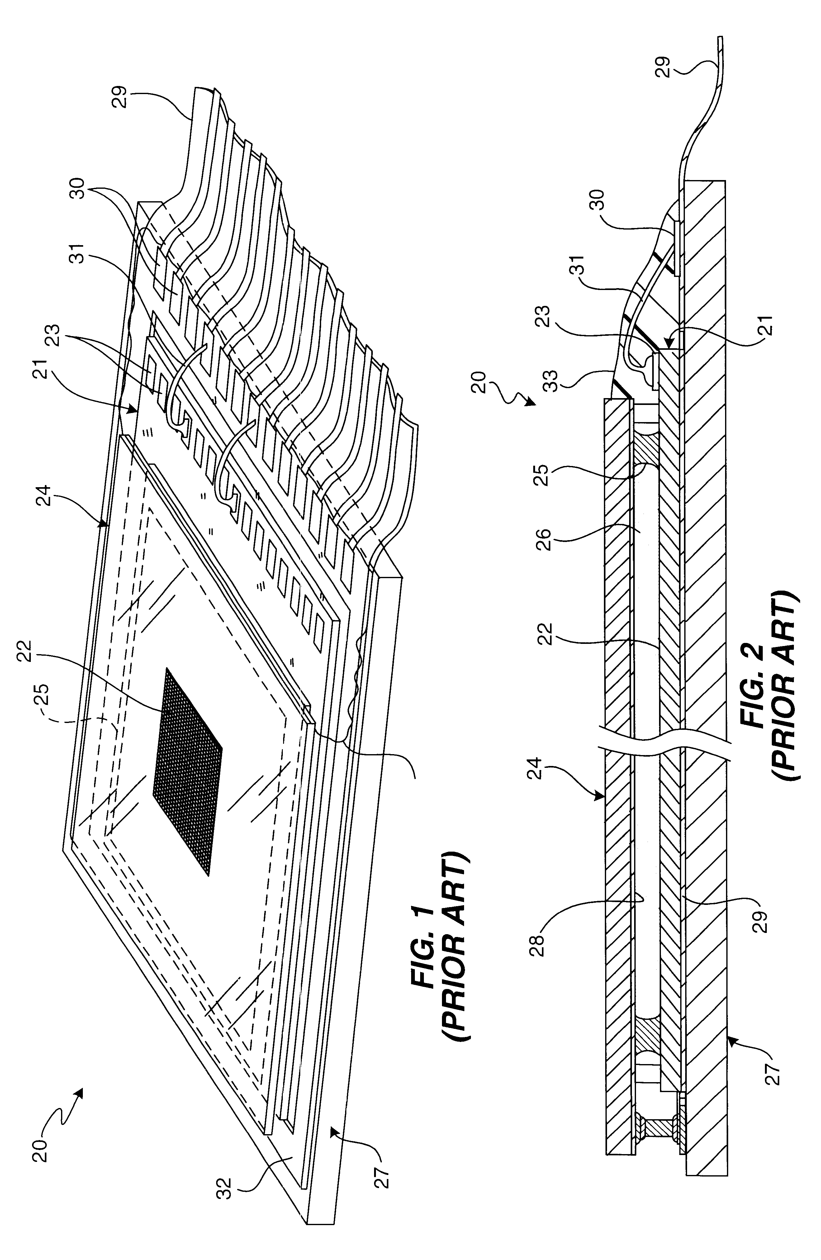
While the present invention will be described with reference to a few specific embodiments, the description is illustrative of the invention and is not to be construed as limiting the invention. Various modifications to the present invention can be made to the preferred embodiments by those skilled in the art without departing from the true spirit and scope of the invention as defined by the appended claims. It will be noted here that for a better understanding, like components are designated by like reference numerals throughout the various figures.

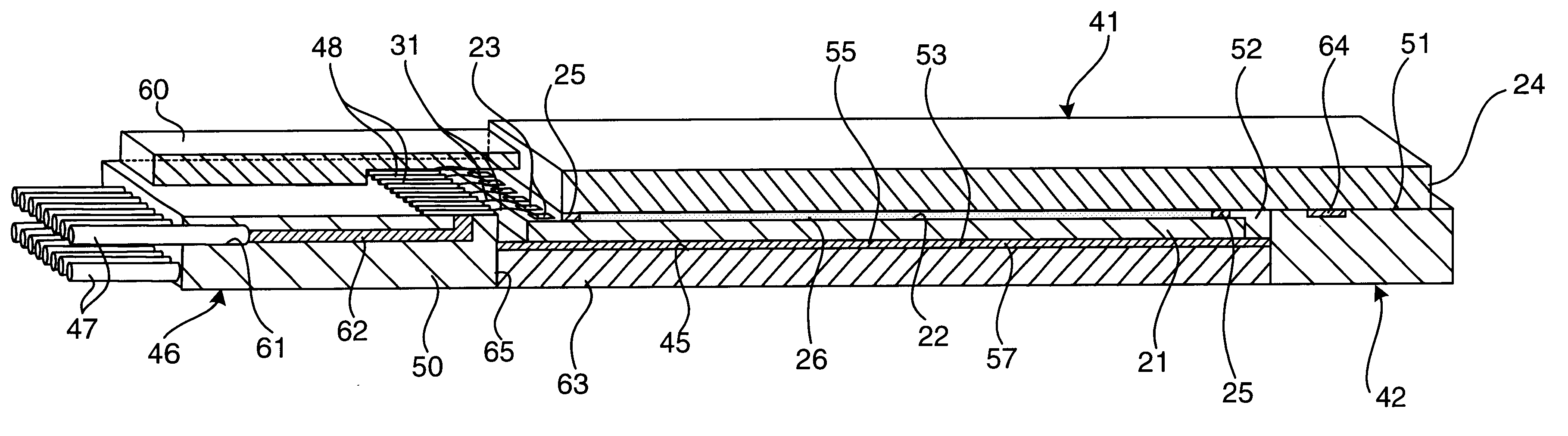
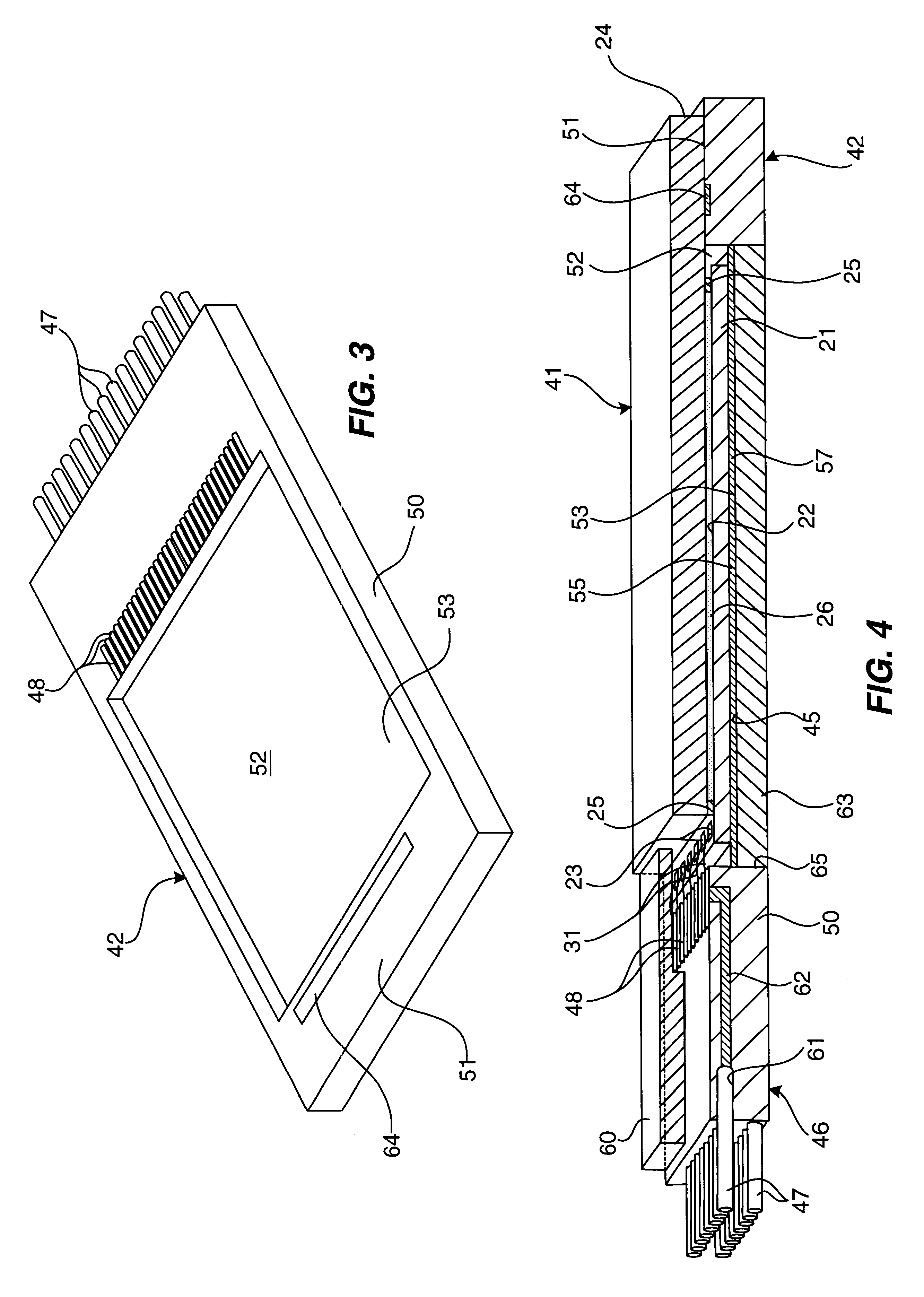
Attention is now directed to FIGS. 3 and 4 where a Liquid Crystal Display package or assembly, generally designated 40, is illustrated including a liquid crystal cell 41 and a containment structure 42. The liquid crystal cell 41 includes a die 21 having a pixel array 22, and a transparent plate 24 attached to the die 21. A liquid crystal material 26 is disposed in a gap region 45 between the die 21 and the transparent plate 24. The conta...


PUM

PropertyMeasurementUnit
temperatureaaaaaaaaaa
transparentaaaaaaaaaa
thermal conductivityaaaaaaaaaa

Abstract

A liquid crystal display package including a liquid crystal cell having a die with a pixel array, and a transparent plate attached to the die. A liquid crystal material is disposed in a gap region between the die and the transparent plate. The display assembly further includes a containment structure adapted to couple to and at least partially receive liquid crystal cell therein, and an electrical connector portion integrated with the containment structure. A plurality of conductive contacts are positioned in the containment structure for secured support thereof, and in substantially stress-free electrical connection with the pixel array. The conductive contacts further are configured to releasably couple to mating conductive contacts of an opposed electrical connector.

Description

The present invention relates, generally, to liquid crystal display assemblies and, more particularly, relates to miniature liquid crystal display assemblies constructed to reduce residual stresses.In the recent past, substantial research and development resources have been directed toward small scale Liquid Crystal Display (LCD) and light valve technologies. These high information content, miniature LCD assemblies enable enhanced availability of graphics, data and video information for employment in high resolution projection displays, such as a reflective LCD projectors, SXGA formats (1,280.times.1,024 pixel resolution) and even HDTV formats (above 1,000 line resolution), or the like.Reflective LCD projectors, in particular, are highly desirable since they offer the brightness of traditional three-lamp front-projection systems in combination with the high resolution of an LCD panel. At the heart of these optical engines is reflective liquid crystal on crystalline silicon light val...

Claims


Application Information

Patent Timeline
Patent Type & Authority Patents(United States)
IPC IPC(8): G02F1/13
CPCG02F1/13452
Inventor MURRAY, G. CADEMATHEW, RANJAN J.
Owner NAT SEMICON CORP
Why Eureka
Try Eureka