Alpha particle shield for integrated circuit

a technology of integrated circuits and shields, applied in the direction of semiconductor devices, semiconductor/solid-state device details, electrical devices, etc., can solve the problems of single event upsets or soft errors

Inactive Publication Date: 2003-03-11
INT BUSINESS MASCH CORP
View PDF15 Cites 19 Cited by
  • Summary
  • Abstract
  • Description
  • Claims
  • Application Information

AI Technical Summary

Problems solved by technology

Integrated circuits are susceptible to alpha particles which may cause single event upsets or soft errors.

Method used


Image

  • Alpha particle shield for integrated circuit
  • Alpha particle shield for integrated circuit
  • Alpha particle shield for integrated circuit

Examples


Embodiment Construction

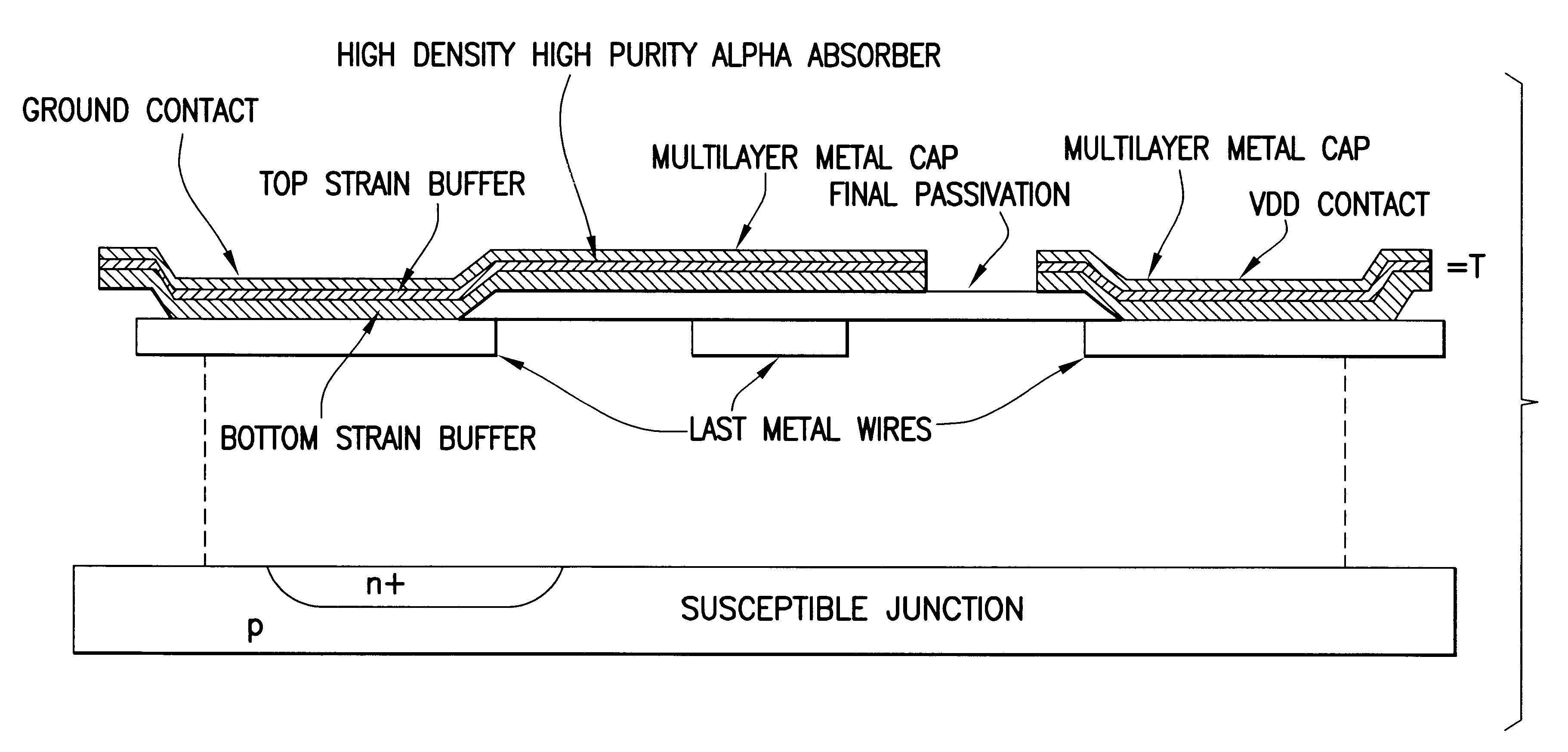
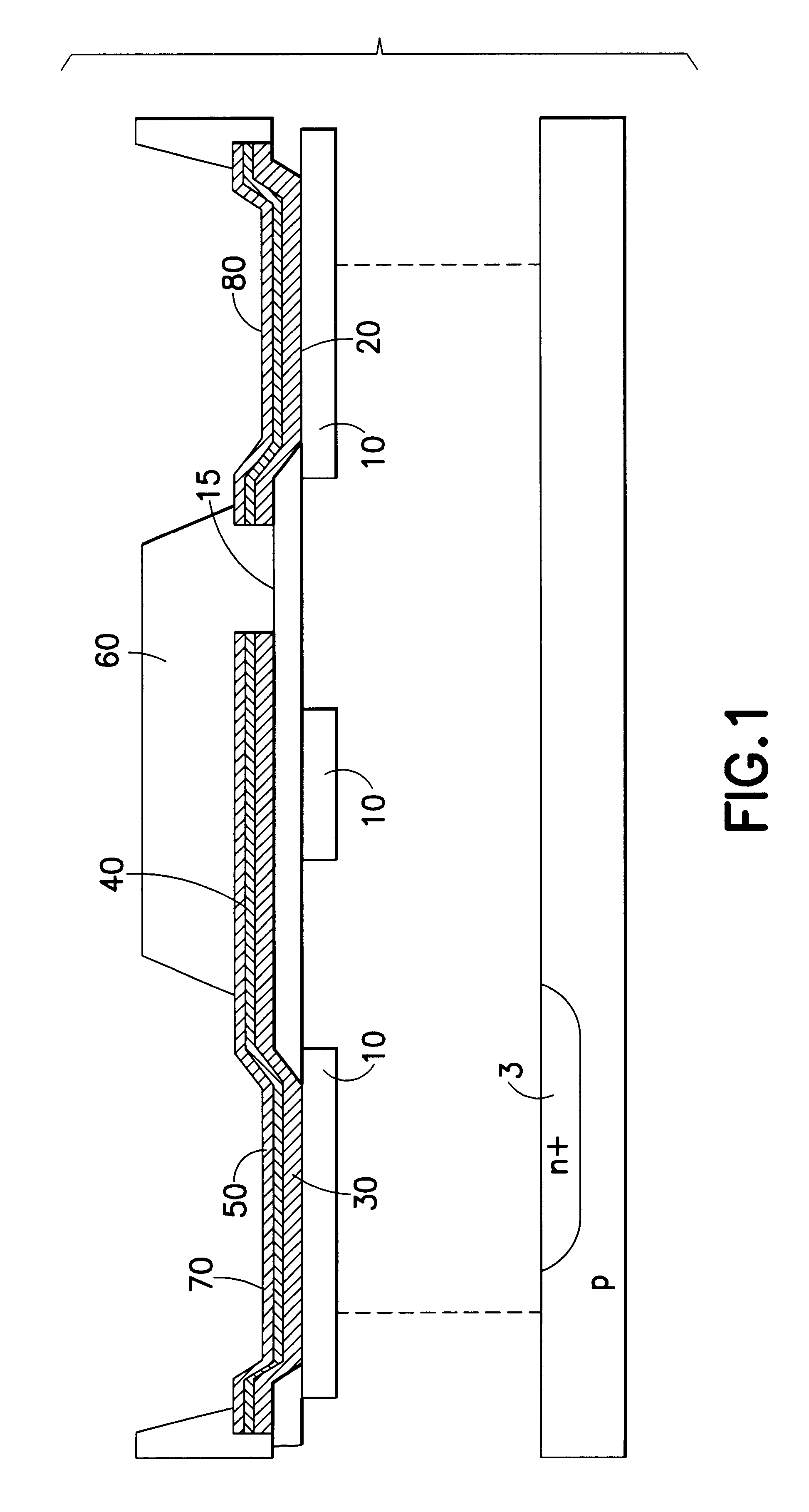
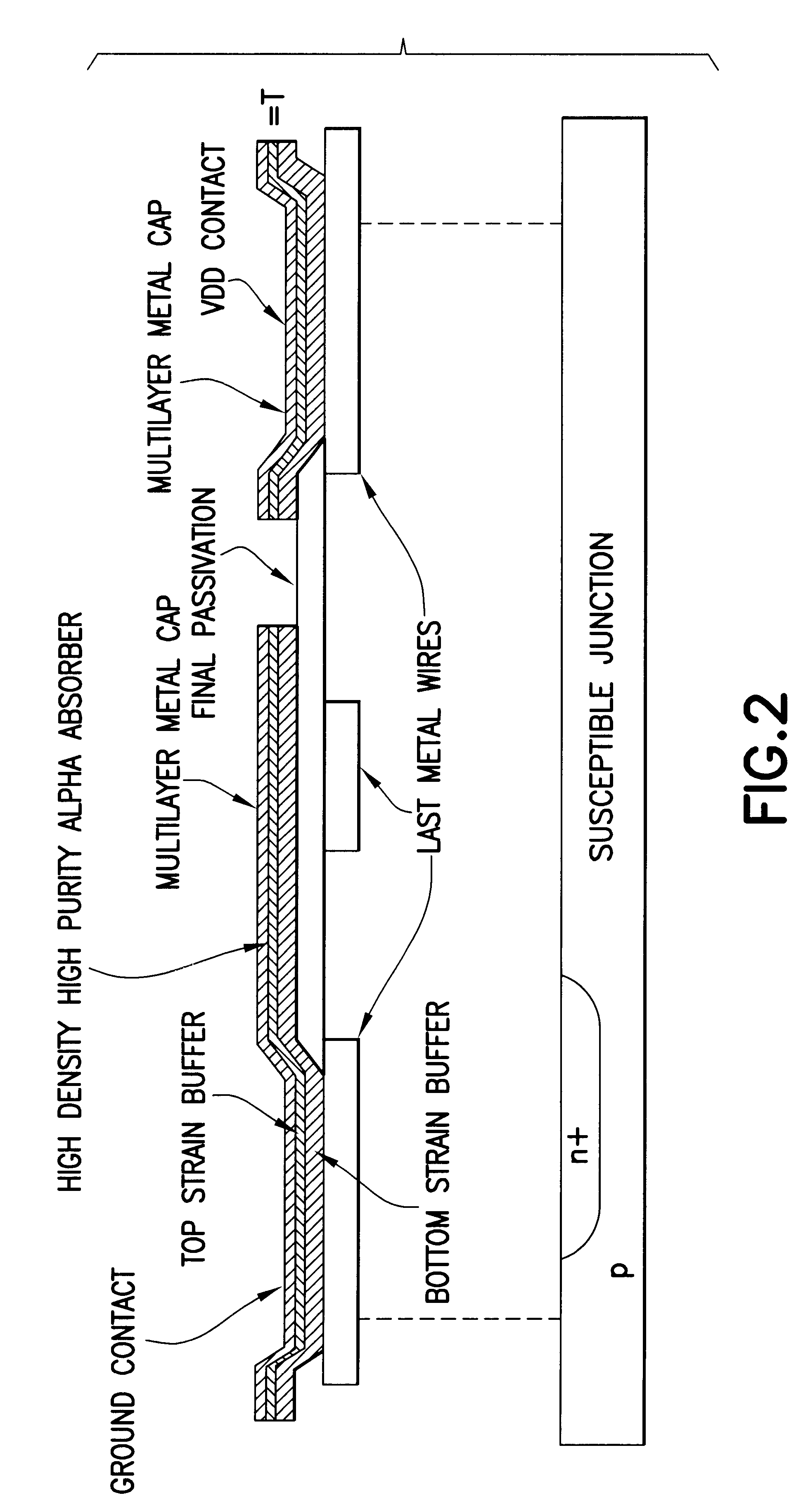
As shown in FIG. 1, the present invention integrates a highly absorbing low alpha particle emission metal layer 40 into a final passivation and terminal metallurgy of an integrated circuit. Aluminum layers 30, 50 provide adhesion and strain buffer layers. An aluminum layer is also transparent to many existing terminal metallurgy processes. The constraints on the choice of metal for the absorbing layer are relaxed by the use of the buffer layer 30 and selection depends primarily on the nuclear properties. These are absorption of alpha particles, absence or minimization of nuclear emissions or fragments which would generate soft errors or single event upset.

The high-purity alpha-particle absorbing non-emitting or low emitting material (metal) may be chosen from the materials Ta, W, Re, Os, or Ir. Other metals or combinations of metal may also be used if they meet the requirements of high purity, no or low alpha-particle emission, and high alpha-particle-absorption. The layer should be...


PUM

PropertyMeasurementUnit
thicknessaaaaaaaaaa
thickaaaaaaaaaa
thickaaaaaaaaaa

Abstract

An integrated circuit, comprising: a semiconductor substrate, a plurality of last metal conductors disposed above said substrate, a bottom metallic layer disposed on said last metal conductors, a top metallic layer, and an alpha absorber disposed between said bottom and top metallic layers, said alpha absorber consisting essentially of a high-purity metal which is an alpha-particle absorber. The metal is, for example, of Ta, W, Re, Os or Ir.

Description

The present invention relates to alpha particle absorbers, and more particularly to such absorbers for integrated circuits.DESCRIPTION OF THE RELEVANT ARTIntegrated circuits are susceptible to alpha particles which may cause single event upsets or soft errors. As is well known, the alpha particles are commonly emitted by the metals, ceramics and other materials associated with a next level of assembly of an integrated circuit.Alpha particle shields for integrated circuits are also known. See, for example, U.S. Pat. No. 6,043,429, METHOD OF MAKING FLIP CHIP PACKAGES, issued Mar. 28, 2000 by Blish, et al. and IBM TECHNICAL DISCLOSURE BULLETIN, 80A 05436, Alpha Particle Shield, pp. 1892-1893, October 1980, which are both incorporated in their entireties herein by reference. Organic shields for alpha particles are also known.The present inventors believe that improvements in alpha particle shields are achievable. According to the present invention, an integrated circuit includes a semic...

Claims


Application Information

Patent Timeline
Patent Type & Authority Patents(United States)
IPC IPC(8): H01L21/02H01L21/60H01L21/70H01L21/768H01L23/556
CPCH01L23/556H01L24/11H01L2924/014H01L2224/13099H01L2924/01013H01L2924/01022H01L2924/01029H01L2924/01042H01L2924/01073H01L2924/01074H01L2924/01075H01L2924/01077H01L2924/01079H01L2924/01082H01L2924/14H01L2924/30105H01L2924/30107H01L2924/3025H01L2924/01005H01L2924/01006H01L2924/01024H01L2924/01033H01L2924/01076
Inventor WACHNIK, RICHARD A.NYE, III, HENRY A.DAVIS, CHARLES R.ZABEL, THEODORE H.RESTLE, PHILLIP J.
Owner INT BUSINESS MASCH CORP
Why Eureka
Try Eureka