Electrical patching system

a technology of patching system and patching panel, which is applied in the field of electrical systems, can solve the problems that conventional patch panels of conventional design do not permit the alteration of signal paths of normalized or grounding circuits

Inactive Publication Date: 2003-03-18
BITTREE
View PDF8 Cites 66 Cited by
  • Summary
  • Abstract
  • Description
  • Claims
  • Application Information

AI Technical Summary

Benefits of technology

Another object of the invention is to provide an apparatus of the aforementioned character in which specially constructed banks of contacts, which are readily accessible from the front of the patch panel, can be selectively interconnected to program a particular circuit to full, half, or non-normal and can also be selectively interconnected to program the grounding of a circuit without costly equipment shutdown and without the necessity of removing the patch panel from the equipment rack.
By way of summary, in the preferred form of the invention, the patch panel comprises a manually programmable device that incorporates shunts or dip switches that are readily accessible from the front panel of the device. In the patch panel construction of the invention, a multi-pin connector block is connected to a first circuit board that, in turn, is connected to a second circuit board via a cable connector, thus allowing the signal switching (normalizing) and grounding circuits of the respective jacks to be selectively altered from the front access panel of the device. By manually changing the shunt or dip switch configurations, the respective normalizing and grounding circuits can easily and simply be altered as may be desired without costly system interruption.

Problems solved by technology

However, prior art patch panels of conventional design do not permit altering of the signal paths of either normalized or grounding circuits without shutting down the system and removing the patch panel from the equipment rack.

Method used


Image

  • Electrical patching system
  • Electrical patching system
  • Electrical patching system

Examples


Embodiment Construction

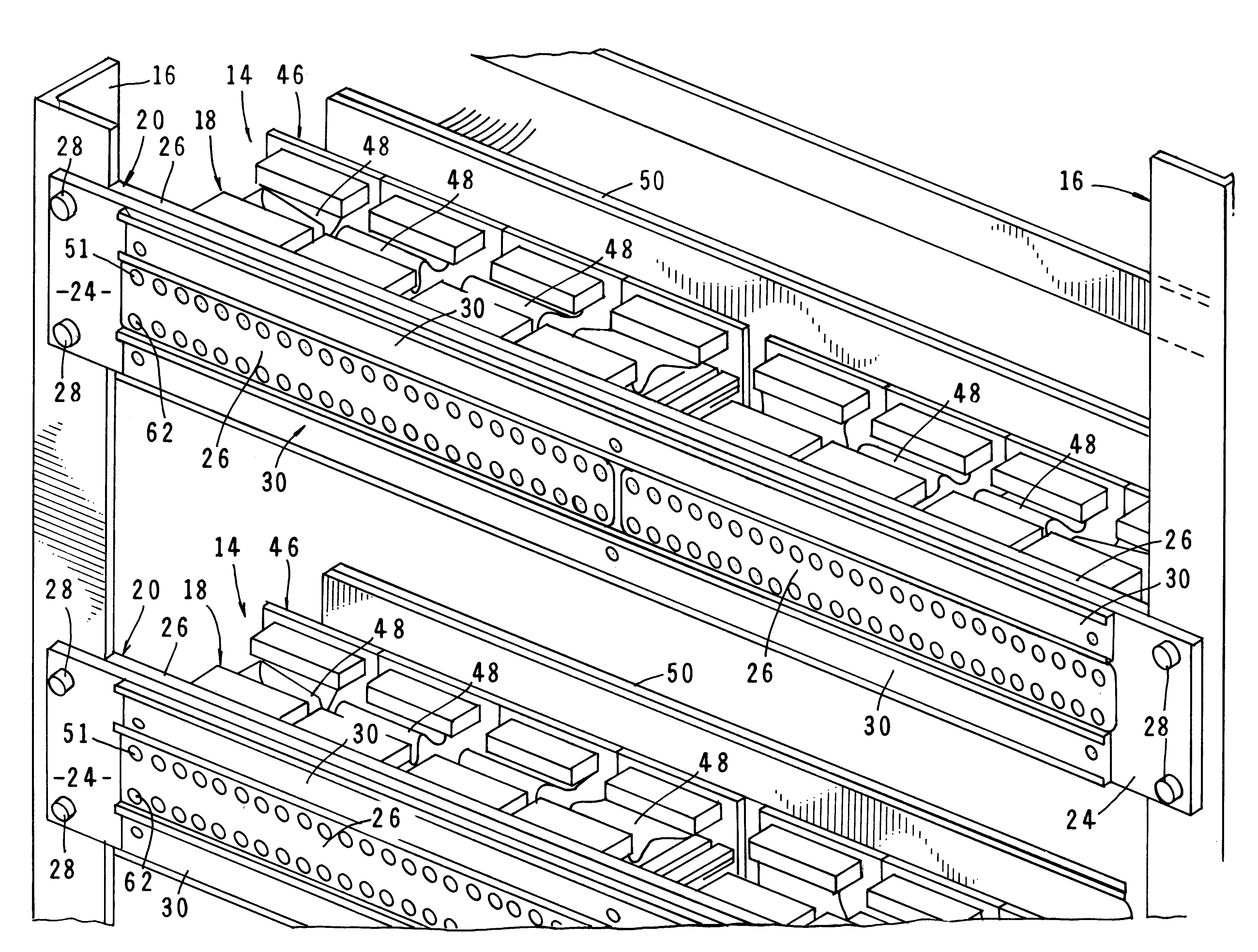
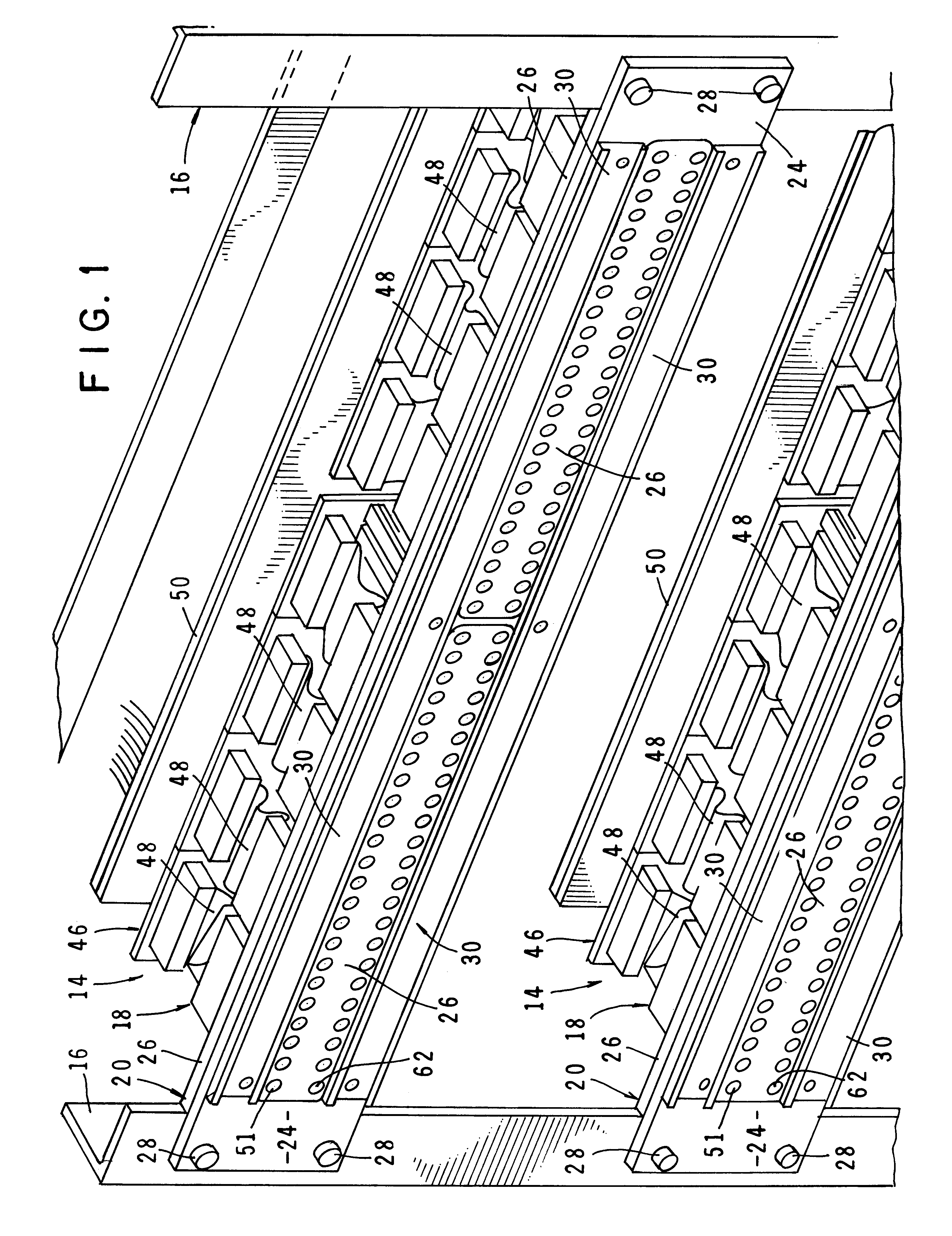
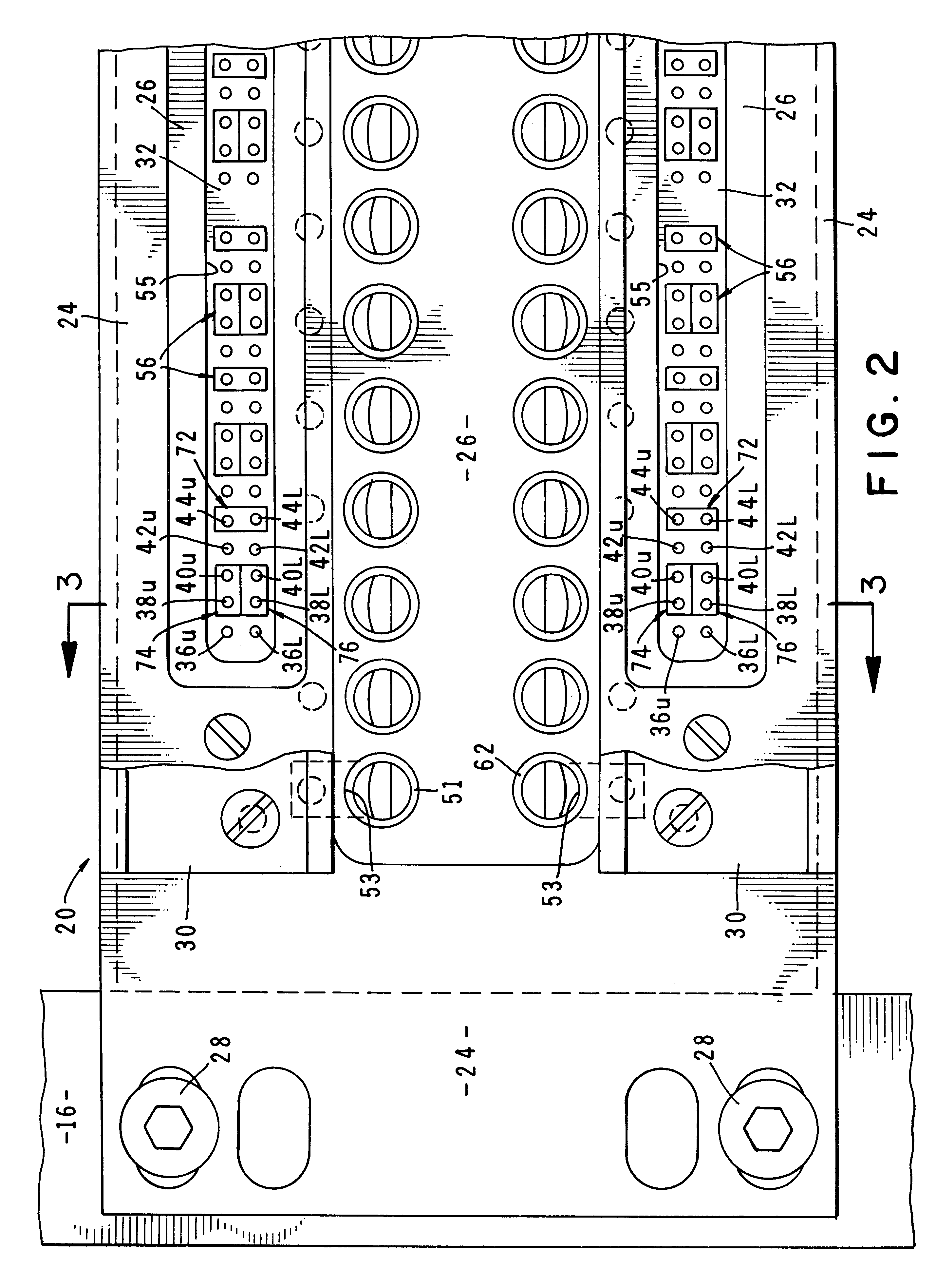
Referring to the drawings and particularly to FIGS. 1, 2 and 3, one form of the programmable patch panel of the invention is there shown. More particularly, FIG. 1 shows a pair of the panels 14 of the invention mounted in a conventional equipment rack 16. As best seen by referring to FIGS. 1 and 3, the patch panels 14 are of identical construction and each comprises a chassis 18 having a front panel assembly 20 that is made up of a front mounting plate 24 and an insulator panel 26. As depicted in FIG. 1, mounting plate 24 is connected to equipment rack 16 by means of threaded connectors 28. Removably connected to each mounting plate 24 is a pair of vertically spaced designation strips 30 that are adapted to carry designation indicia that identify the various electrical circuits carried by chassis 18.

Connected to the insulator panel of each of the patch panels 14 is a circuit board 32 having a plurality of circuits to which a plurality of transversely spaced apart ten-pin header asse...


PUM


Abstract

By way of summary, in the preferred form of the invention, the patch panel comprises a manually programmable device that incorporates shunts or dip switches that are readily accessible from the front panel of the device. In the patch panel construction of the invention, a multi-pin connector block is connected to a first circuit board that, in turn, is connected to a second circuit board via a cable connector, thus allowing the signal switching (normalizing) and grounding circuits of the respective jacks to be selectively altered from the front access panel of the device. By manually changing the shunt or dip switch configurations, the respective normalizing and grounding circuits can easily and simply be altered as may be desired without costly system interruption.

Description

1. Field of the InventionThe present invention relates generally to electrical systems. More particularly, the invention concerns a patching device for use in connection with communication systems that permits altering the signal flow paths within selected normalizing and grounding circuits of the communication system from the front panel of the patching device.2. Discussion of the Prior ArtElectrical patching equipment is widely used in a variety of different applications for selectively connecting and disconnecting electrical circuits. By way of example, electrical patching equipment is frequently used to make selected circuit connections between a number of types of electrical equipment. More particularly, present day professional communication systems, which include telecommunication, production, post-production, media storage and other devices utilizing transmission equipment, typically embody patch panels for temporarily connecting various circuits. A patch panel or patch boar...

Claims


Application Information

Patent Timeline
Patent Type & Authority Patents(United States)
IPC IPC(8): H01R31/08H01R29/00H01R31/00H04Q1/02H04Q1/14
CPCH01R29/00H01R31/08H04Q1/13H04Q1/116H01R23/68H04Q2201/14H04Q2201/12H01R12/73H01R12/79
Inventor CARPENTER, BRYAN J.GARRARD, GLEN
Owner BITTREE
Why Eureka
Try Eureka