

Imaging device for digital photography
a technology for imaging devices and digital photography, applied in the field of digital photography, can solve the problems of unsuitable as a complete replacement for films, unsuitable for the large selection of commercially available camera bodies, and limited to camera bodies
- Summary
- Abstract
- Description
- Claims
- Application Information
AI Technical Summary
Benefits of technology
Problems solved by technology
Method used
Image

Examples
Embodiment Construction
The description hereinbelow is made in reference to 35 mm photographic systems. This is made in a way of example and it does not limit the scope of the invention.
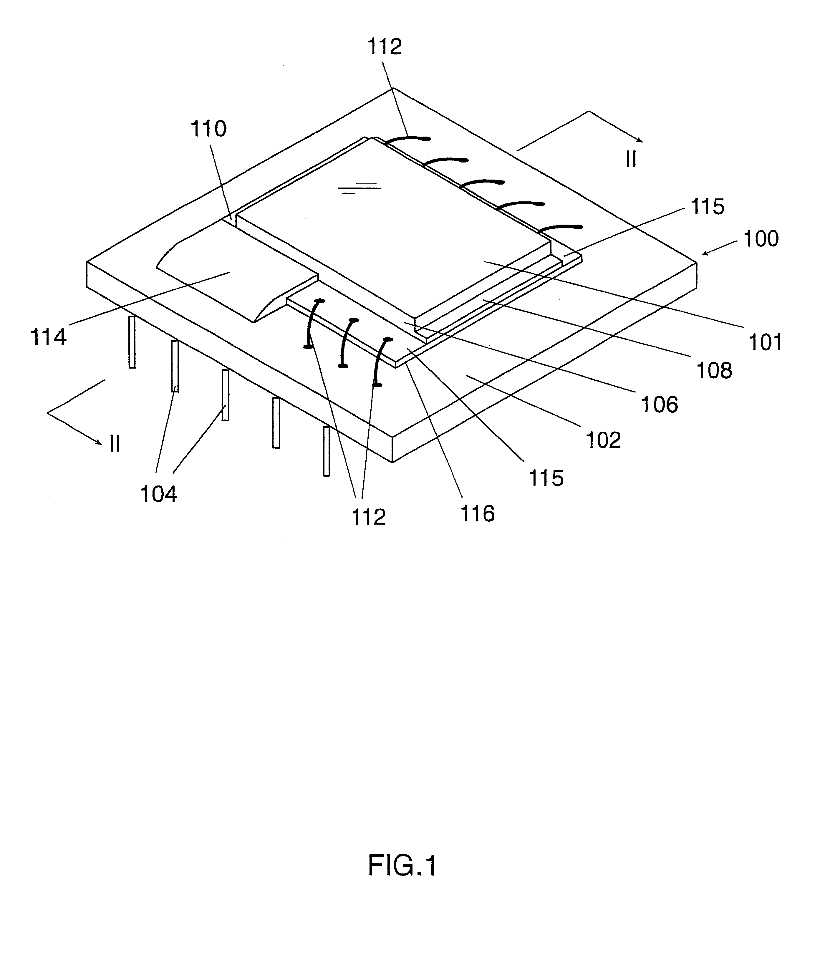
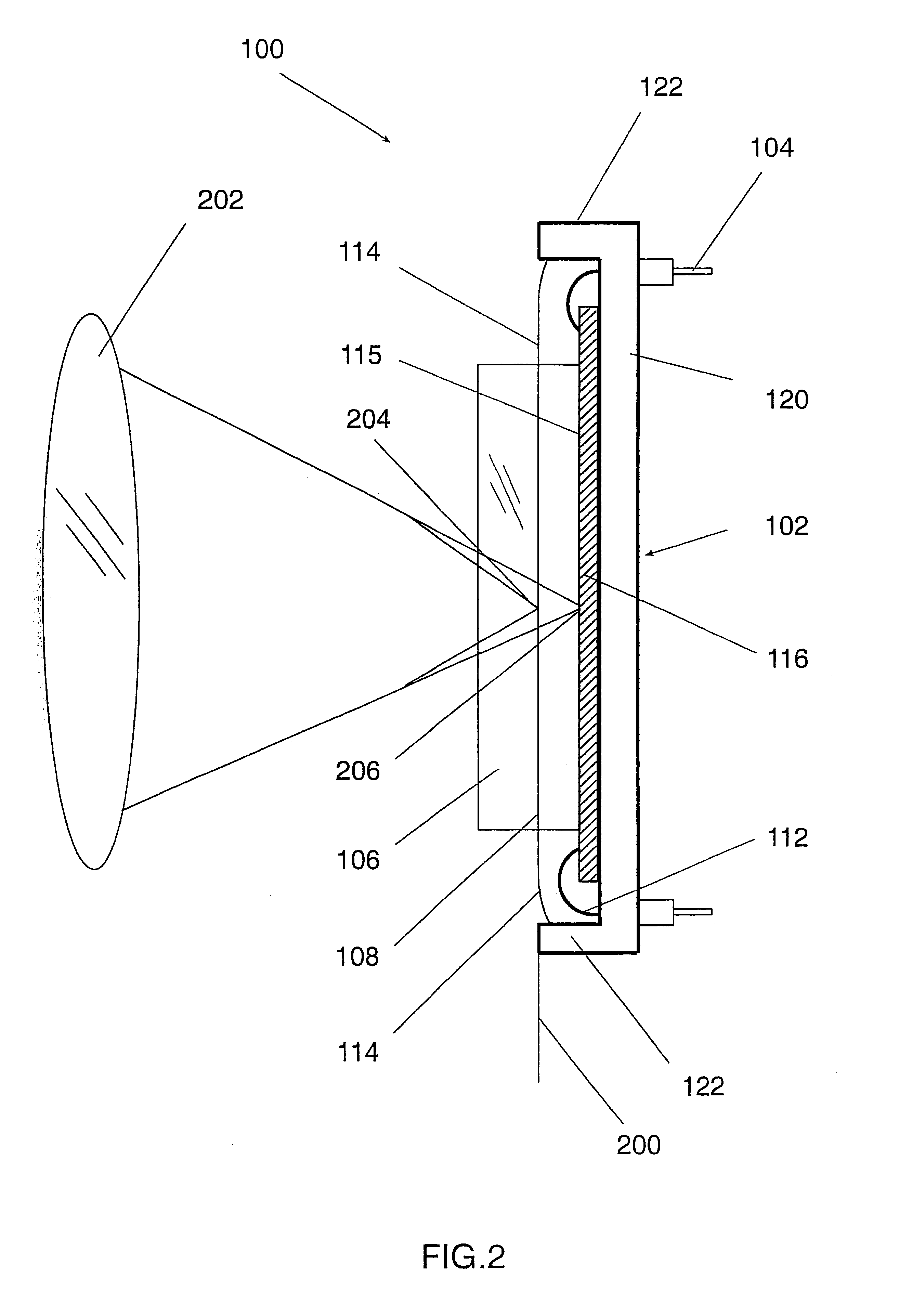
Reference is made to FIG. 1, which is a general schematic view of an imaging device, generally designated 100, in accordance with a preferred embodiment of the invention.
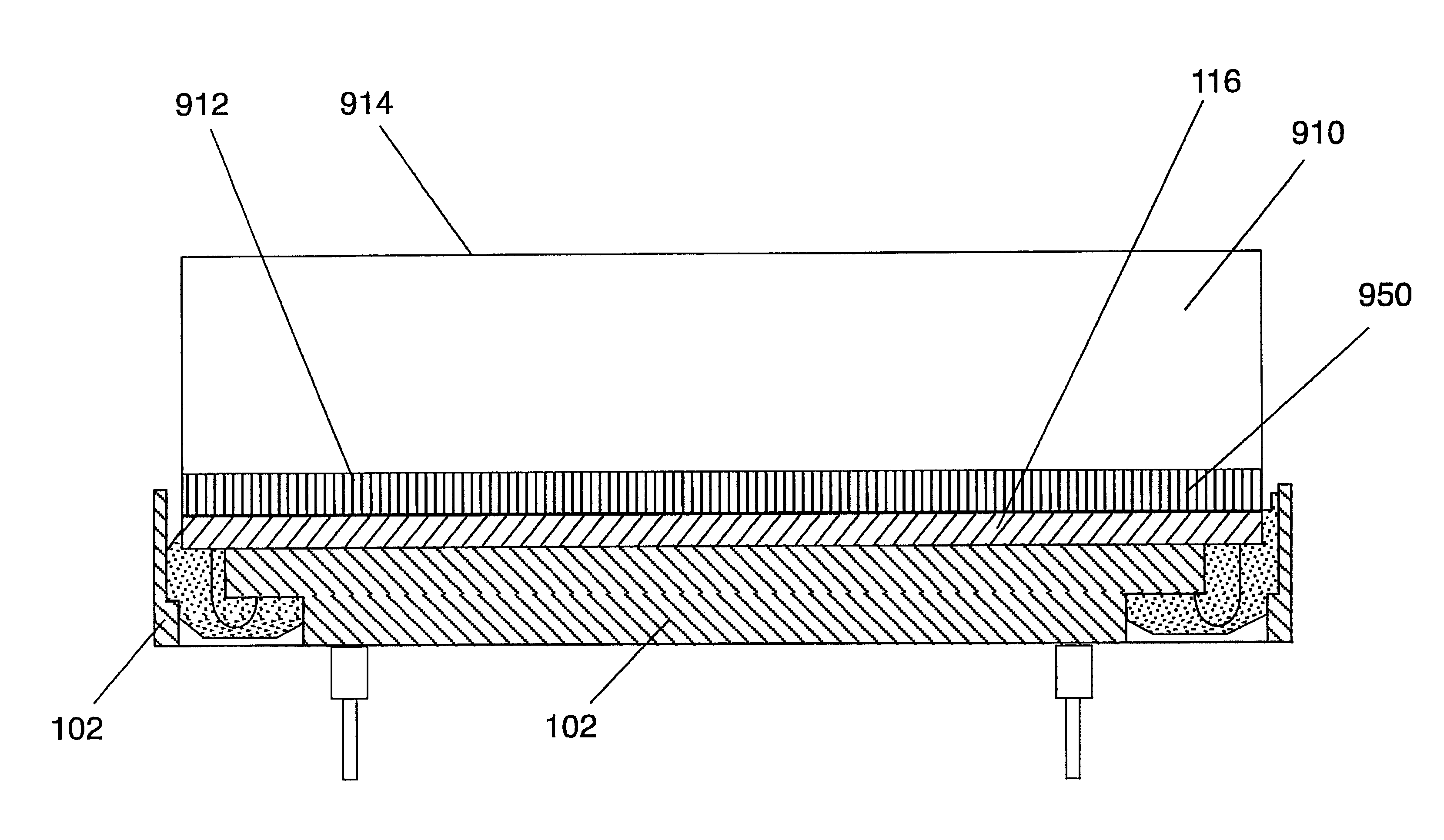
Imaging device 100 comprises a glass cover 106, having two leading edges, referenced 108 and 110, which are glued directly to the upper surface 115 of a semiconductor die 116. The two leading edges, referenced 108 and 110, are parallel to the longer (36 mm) side of the die 116. Any suitable glue, such as glues used for gluing doublets in optical systems may be used. Glass cover 106 is generally concentric with the sensitive area, referenced 101, of die 116.
The imaging device sensitive area 101 of the imaging device 100, is configured to match the size of a standard 35 mm format, that is 24 mm.times.36 mm. The glass cover 106 is approximately 35 mm long (alo...
PUM
 Abstract
Description
Claims
Application Information