Multiple input phase lock loop with hitless reference switching
a reference switching and input phase lock technology, applied in the field of digital timing circuits, can solve the problems of reducing the maximum size of the phase excursion, affecting the operation of the output clock, and generating phase perturbations on the output clock
- Summary
- Abstract
- Description
- Claims
- Application Information
AI Technical Summary
Benefits of technology
Problems solved by technology
Method used
Image
Examples
Embodiment Construction
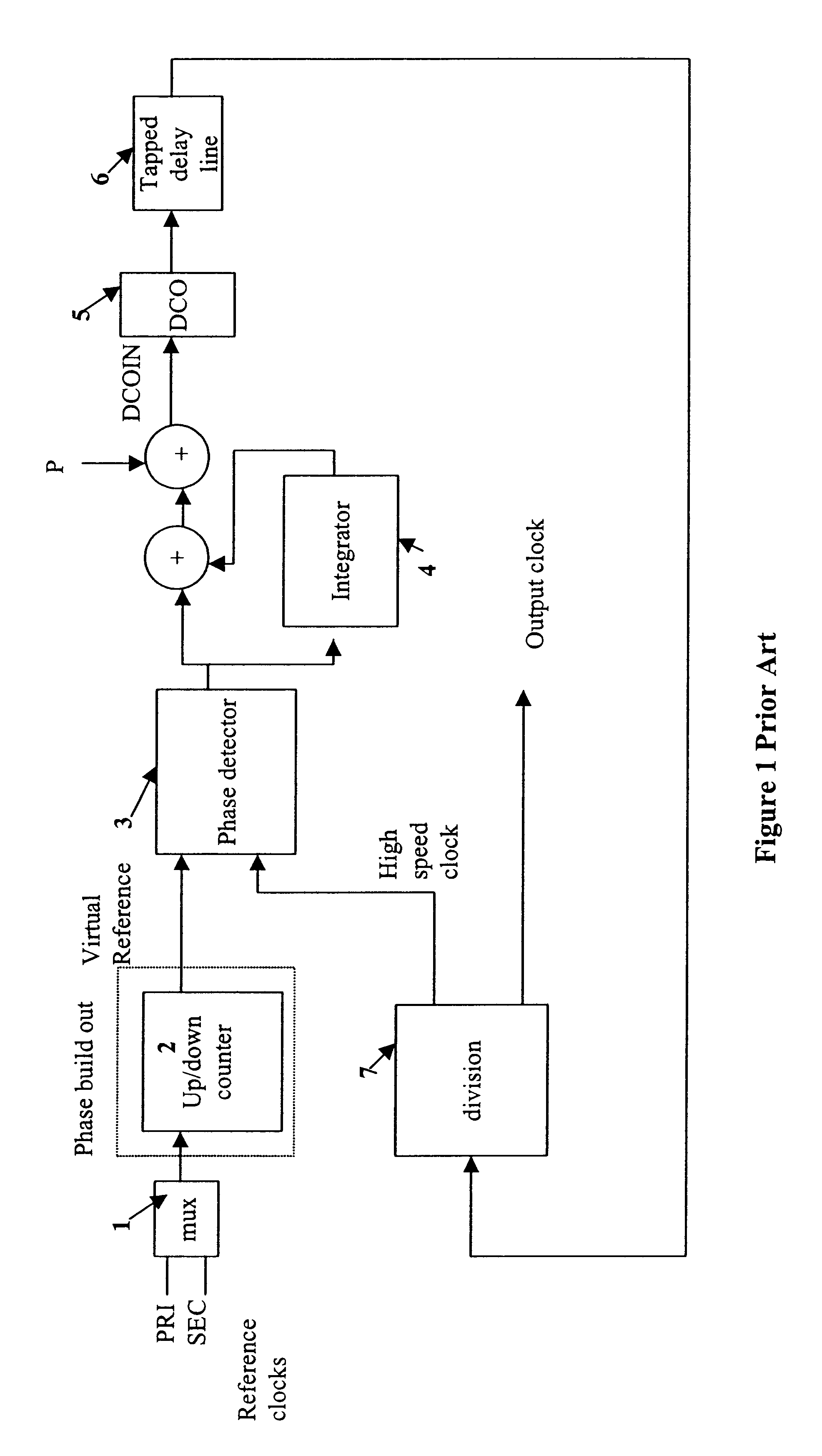
The prior art phase locked loop shown in FIG. 1 comprises a mux 1 selecting between two possible input reference clocks "pri" and "sec", a counter 2 that calibrates and builds out the phase difference between the two clocks upon reference switching, a phase detector 3 receiving a reference signal in, an integrator 4, a digital controlled oscillator 5 for generating an output signal at a desired frequency and a control signal representing the time error in the output signal, a tapped delay line 6 for receiving the output signal of the digital controlled oscillator 5, the tapped delay line 6 producing an output signal from a tap determined by said control signal, and a divider circuit 7 generating a feed back signal for the second input of the phase detector 3 and a synchronous high speed clock to the phase build out counter 2. The function of the integrator 4 is to eliminate input to output phase variations that would otherwise occur due to differences in the reference clock center f...
PUM
 Abstract
Description
Claims
Application Information


