Delay locked loop

a technology of locking loop and delay, which is applied in the direction of digital storage, pulse automatic control, generating/distributing signals, etc., can solve the problems of deteriorating performance of correcting duty errors in the dll, hard to precisely correct the duty cycle, and inevitable generation of delay between the external clock and the internal clock. , to achieve the effect of reducing jitter and reducing jitter

Inactive Publication Date: 2007-10-16
SK HYNIX INC
View PDF20 Cites 48 Cited by
  • Summary
  • Abstract
  • Description
  • Claims
  • Application Information

AI Technical Summary

Benefits of technology

[0013]It is, therefore, an object of the present invention to provide a delay locked loop (DLL) for reducing jitter during a high frequency operation by separately controlling a coarse delay and a fine delay.
[0014]In accordance with an aspect of the present invention, there is provided a DLL for reducing jitter, including: a multiplexing unit for receiving an external clock and an inverted external clock to generate a rising clock and a falling clock having an inverse phase of the rising clock, and selectively outputting one of the rising clock and the falling clock according to a first phase comparing signal; a first delay line for generating a first internal clock by delaying an output clock of the multiplexing unit for a certain time, and generating a second internal clock by delaying the first internal clock for a determined time, in response to the first phase comparing signal and a second phase comparing signal; a delay line control unit for generating an enable signal whose activation is controlled by a phase difference between the rising clock and the falling clock when a duty cycle correction mode enters; a second delay line for generating a first clock by delaying the first internal clock for a predetermined time, and generating a second clock by delaying the second internal clock for a preset time, under the control of the enable signal; a phase control unit for outputting a plurality of mix control signals by comparing a phase of the first clock with a phase of the second clock, and generating a first DLL clock and a second DLL clock by mixing the phases of the first clock and the second clock in response to the plurality of the mix control signals; and a phase comparing unit for generating the first phase comparing signal and the second phase comparing signal by comparing a phase of the first DLL clock and the second DLL clock with a phase of the rising clock, and generating a lock signal for controlling an operation timing of the first delay line and the second delay line.

Problems solved by technology

When the external clock is used in the internal circuit, a delay is inevitably generated between the external clock and an internal clock.
In the conventional DLL, it is possible to adjust a delay of whole phases by using the reference clock REF and the feedback clock FB, but it is hard to exactly correct the duty cycle.
Moreover, in case of a duty cycle correction (hereinafter, referred to as a DCC) operation, a performance for correcting the duty error in the DLL is deteriorated because a mixed input signal is variable according to a voltage level of an external source voltage.
As a result, jitter appears in the DLL of the DRAM.

Method used


Image

  • Delay locked loop
  • Delay locked loop
  • Delay locked loop

Examples


Embodiment Construction

[0030]Other objects and aspects of the invention will become apparent from the following description of the embodiments with reference to the accompanying drawings, which is set forth hereinafter.

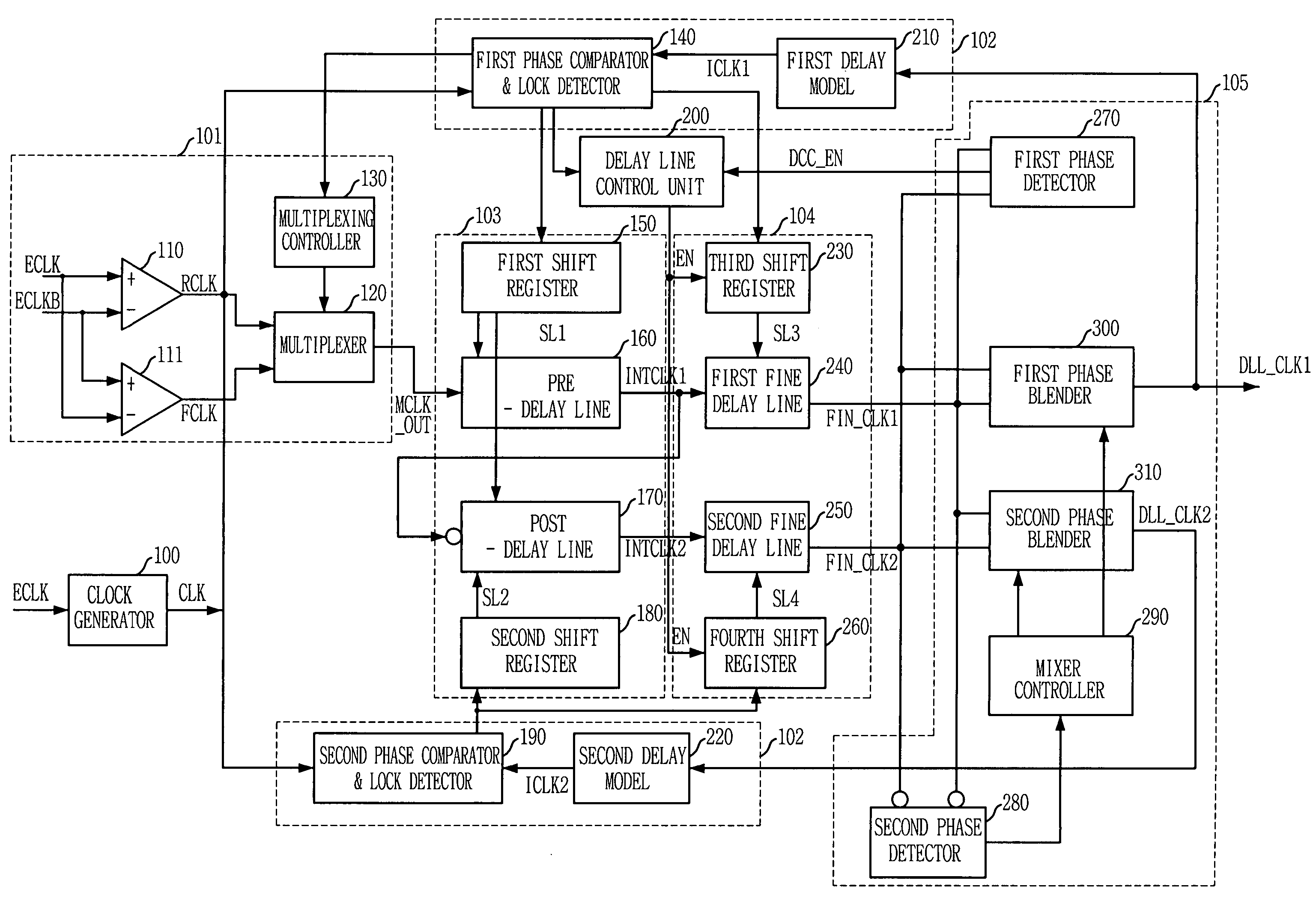
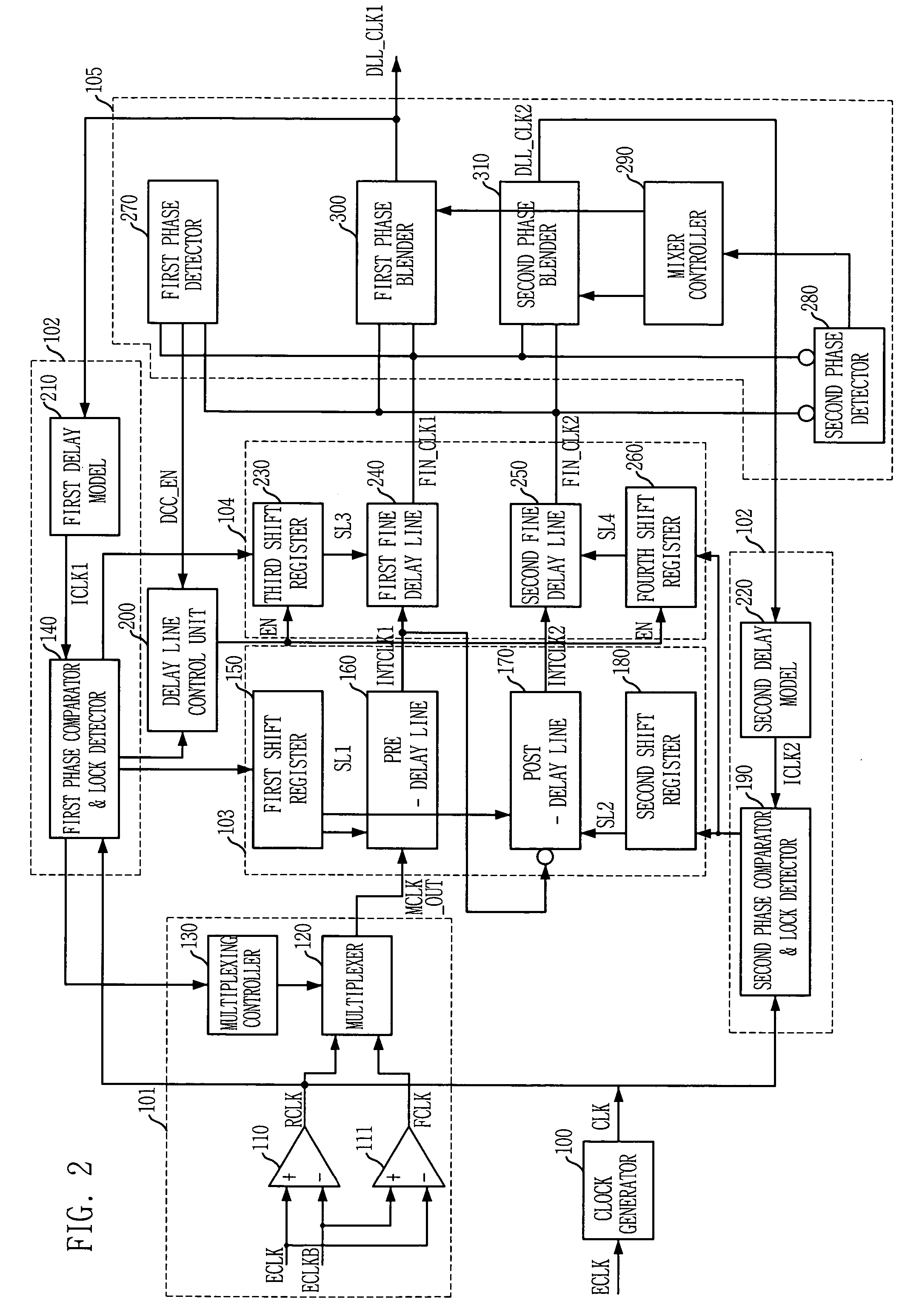
[0031]FIG. 2 is a block diagram showing a delay locked loop (DLL) of a semiconductor memory device in accordance with an embodiment of the present invention.

[0032]As shown, the DLL in accordance with an embodiment of the present invention includes a clock generating unit 100, a multiplexing unit 101, a phase comparing unit 102, a first delay line 103, a second delay line 104, a phase control unit 105, and a delay line control unit 200.

[0033]Herein, the multiplexing unit 101 includes a first clock buffer 110, a second clock buffer 111, a multiplexer 120 and a multiplexing controller 130. The phase comparing unit 102 includes a first phase comparator & lock detector 140, a second phase comparator & lock detector 190, a first delay model 210 and a second delay model 220. The first delay line 1...


PUM


Abstract

A DLL for reducing jitter during a high frequency operation by separately controlling a coarse delay and a fine delay. The DLL includes a multiplexing unit for selectively outputting one of the rising clock and the falling clock; a first delay line for generating a first internal clock and a second internal clock; a second delay line for generating a first clock and a second clock; a delay line control unit for controlling the second delay line; a phase control unit for generating a first DLL clock and a second DLL clock by mixing the first clock and the second clock; and a phase comparing unit for comparing the first DLL clock and the second DLL clock with the rising clock to generate a lock signal for controlling an operation timing of the first delay line and the second delay line.

Description

FIELD OF THE INVENTION[0001]The present invention relates to a delay locked loop; and more particularly, to a delay locked loop (DLL) for reducing jitter during a high frequency operation by separately controlling a coarse delay and a fine delay.DESCRIPTION OF RELATED ART[0002]As a semiconductor memory device operates with high speed, a delay locked loop (hereinafter, referred to as a DLL) device is used for synchronizing an internal clock with an external clock in the semiconductor memory device. When the external clock is used in the internal circuit, a delay is inevitably generated between the external clock and an internal clock. Accordingly, the DLL device is used for compensating a clock skew, which is a difference between the internal clock and the external clock. Namely, the DLL device synchronizes the internal clock with the external clock by controlling the clock skew.[0003]An operation speed of a dynamic random access memory (hereinafter, referred to as a DRAM) increases,...

Claims


Application Information

Patent Timeline
Patent Type & Authority Patents(United States)
IPC IPC(8): H03L7/06G06F1/04G06F1/10G11C11/407G11C11/4076H03K5/00H03K5/04H03K5/13H03K5/131H03L7/081
CPCH03L7/0814H03L7/0818H03L7/087H03L7/0816H03L7/00H03L7/08
Inventor LEE, HYUN-WOO
Owner SK HYNIX INC
Why Eureka
Try Eureka