Method of forming defect-free ceramic structures using thermally depolymerizable surface layer

a technology of depolymerizable surface layer and ceramic structure, which is applied in the direction of basic electric elements, manufacturing tools, solid-state devices, etc., can solve the problems of increasing circuit density, corresponding increase in overall manufacturing problems, and process improvements alone are not sufficient to eliminate all random defects affecting yield and reliability, so as to achieve the effect of reducing and/or eliminating processing defects

Inactive Publication Date: 2003-07-22
INT BUSINESS MASCH CORP
View PDF15 Cites 13 Cited by
  • Summary
  • Abstract
  • Description
  • Claims
  • Application Information

AI Technical Summary

Benefits of technology

The present invention is a novel method and structure for providing at least one sacrificial protective polymer adhesive layer over a green sheet laminate in order to minimize and / or eliminate processing defects. The surface protective film preferably comprises of at least one thermally depolymerizable polymer which cleanly burns off during the sintering cycle.
(a) adhesive bonding to ceramic laminates during high pressure lamination process which bonding is maintained during sizing and dicing operations providing excellent protection for ceramic and thus minimizing yield loss which otherwise occurs due to defects caused by flying debris landing on the surface of ceramic;

Problems solved by technology

However, increase in circuit density produce a corresponding increase in overall manufacturing problems.
Whereas significant improvements are being made to eliminate systematic defects by reducing process variability, process improvements alone are not sufficient to eliminate all the random defects which effect both yield and reliability.
These high performance chips have a large number of external inputs / outputs (I / Os), such as pads or solder balls, to name a few, and these chips have a very high power dissipation requirement.
Such defects in the ceramic substrates are undesirable and thus significant number of sintered substrates have to be reworked or discarded causing additional expenses and / or product yield losses.

Method used


Image

  • Method of forming defect-free ceramic structures using thermally depolymerizable surface layer
  • Method of forming defect-free ceramic structures using thermally depolymerizable surface layer
  • Method of forming defect-free ceramic structures using thermally depolymerizable surface layer

Examples


example 1

Several samples of the multilayer ceramic structures having defect-free surface metallurgical features were fabricated using the process of this invention.

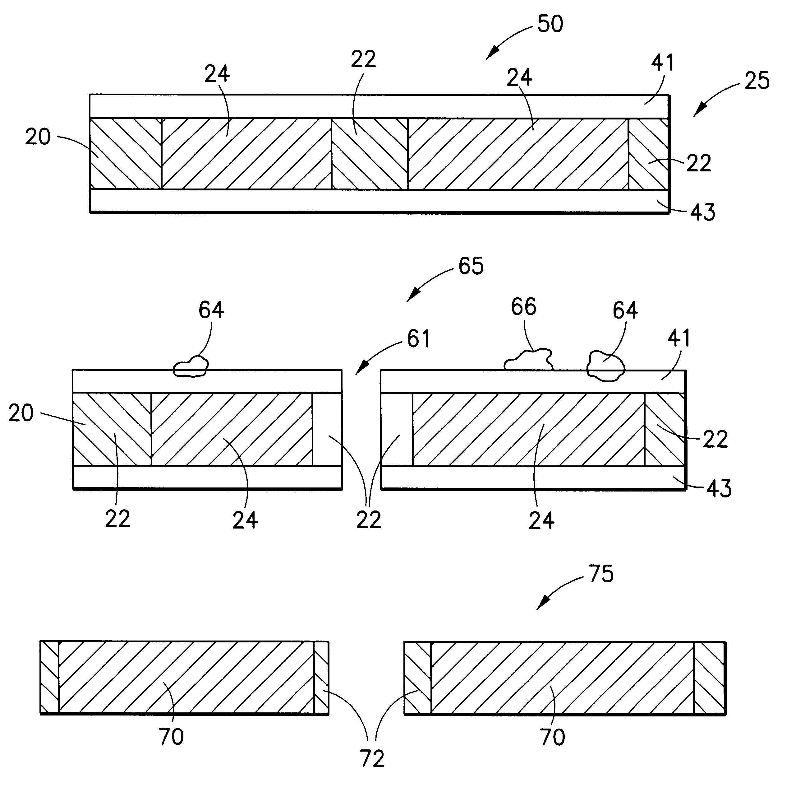
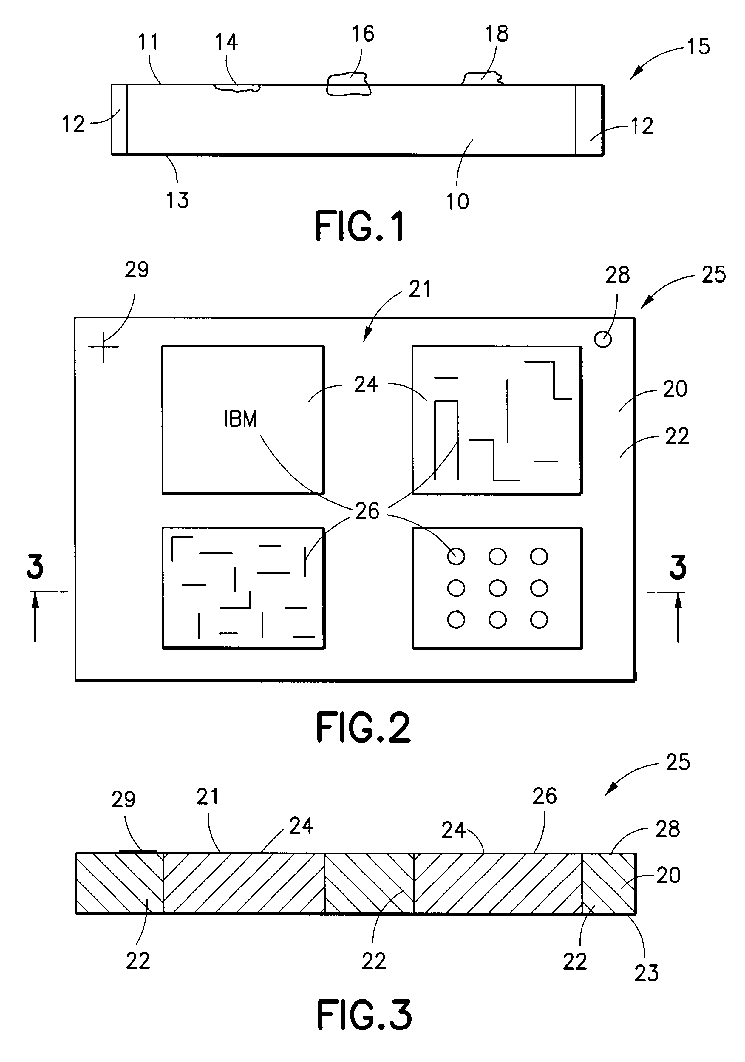
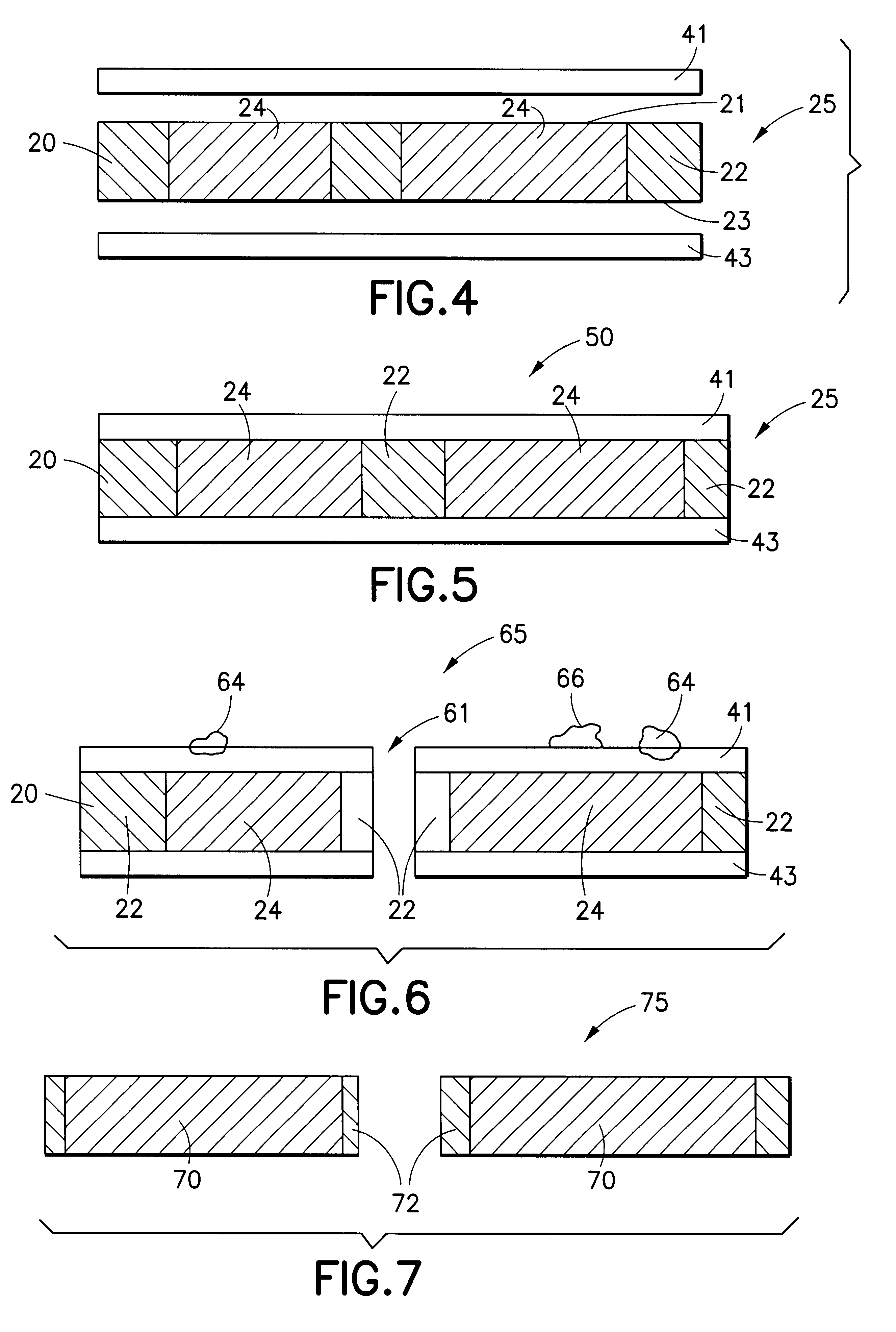
In one sample a stack containing metallized ceramic layers 24, was placed in a lamination frame (not shown). A polyacrylate based thermoplastic adhesive film QL3500 having thickness of about 1-2 mil, was then placed over the top and bottom surface of the stack. The protective adhesive thermoplastic film 41 and / or 43, which had a thickness of about 1-2 mil, was obtained from DuPont and was found to have an elongation of about 200 percent at room temperature.

This assembly was then placed inside a 3 mil thick polyurethane bag (durometer 30 shore A), evacuated and heat sealed. The polyurethane bag, was obtained from Stevens Urethane Film & Sheet, Northampton, Mass., USA. The bag, with its contents were then laminated under pressure to about 5000 psi and at a temperature to about 90.degree. C. in an isostatic press.

After the lamination...

example 2

In another set of samples the assembly of ceramic layers stack 25, was laminated in a manner described in Example 1, but no thermally depolymerizable surface layer was used. These samples had embedded surface debris and bonded green sizing debris and showed severe paste and ceramic pull by the bag material and also by the lamination plate. This demonstrated the need for the sacrificial protective interface layer 41 and / or 43, and the process of this invention.

example 3

In another series of samples, different type of polyacrylate based thermally decomposable surface films, LF0100 and LF0200 films of 1-2 mil thickness, commercially available from DuPont as a family of Pyralux products were used. Basically, the assembly of metallized ceramic layers were stacked and placed in the lamination frame, as described in Example 1.

Other polyacrylates derived thermally depolymerizable / decomposable films tried were made of homopolymers, co-polymers, terpolymers, or physical mixtures thereof, of derived from acrylic monomers. The desired characteristics of these decomposable thermoplastic films include a thickness in the range of about 1 mil to about 5 mils and elongation varying between 150 percent to about 550 percent, with elastic modulus being about 0.3 GPa.

The rest of the assembly and the procedure followed was similar to the one explained in Example 1. Again, there was no evidence of fused debris on the metallurgical features and no paste pull-outs was see...


PUM

PropertyMeasurementUnit
elongation-at-breakaaaaaaaaaa
glass transition temperatureaaaaaaaaaa
Tgaaaaaaaaaa

Abstract

This invention relates generally to a new method of forming semiconductor substrates with defect-free surface metallurgical features. In particular, the invention related to a method for providing surface protected ceramic green sheet laminates using at least one thermally depolymerizable surface layer. More particularly, the invention encompasses a method for fabricating semiconductor substrates wherein a thermally depolymerizable / decomposable surface film is placed over a ceramic green sheet stack or assembly prior to lamination and caused to conform to the surface topography of the green sheet during lamination. The invention also encompasses a method for fabricating surface protected green sheet laminates which can be sized or diced without causing process related defects on the ceramic surface. After lamination the thermally depolymerizable / decomposable film is conveniently and cleanly removed due to thermal depolymerization and burn-off of volatile species during the sintering process, thus providing surface defect-free ceramic substrates.

Description

The present invention relates generally to a method and a structure for forming semiconductor substrates, and particularly relates to improvement in ceramic manufacturing process and structure for the production of ceramic packages using at least one thermally depolymerizable surface layer. More particularly, this invention relates to ceramic green laminate processing and structure using at least one protective overlay that adheres to at least a portion of the green ceramic surface to provide reduction / elimination of defects caused during processing, such as, handling and sizing / dicing operations.Semiconductor substrates and devices are becoming smaller and more dense with the evolution of new technologies. However, increase in circuit density produce a corresponding increase in overall manufacturing problems. These manufacturing problems must however be kept to a minimum in order for the semiconductor manufacturer to remain competitive. The semiconductor manufacturers are therefore...

Claims


Application Information

Patent Timeline
Patent Type & Authority Patents(United States)
IPC IPC(8): H01L23/48H01L21/48H01L21/02H01L23/498B28B11/14H01L23/12H05K3/46
CPCH01L21/481H01L23/49894H01L2924/09701H01L2924/12044Y10S438/976H01L2924/0002H01L2924/00
Inventor NATARAJAN, GOVINDARAJANINDYK, RICHARD F.PETERSON, VINCENT P.SACHDEV, KRISHNA G.
Owner INT BUSINESS MASCH CORP
Why Eureka
Try Eureka