Nonvolatile memory circuit for recording multiple bit information

a memory circuit and non-volatile technology, applied in static storage, digital storage, instruments, etc., can solve the problems of inability to accurately perform the read-out of the cell transistor m1, inability to achieve high reliability, and loss of all the electronic components of the floating ga

Inactive Publication Date: 2003-09-02
SPANSION INC +1
View PDF5 Cites 58 Cited by
  • Summary
  • Abstract
  • Description
  • Claims
  • Application Information

AI Technical Summary

Problems solved by technology

Due to the fact that the floating gate of such widely used non-volatile memories is conductive, when defects, however small, are present in the gate oxide film, electrons in the floating gate are all lost via these defects and there is a problem in that high reliability is unattainable.
Moreover, through selection of the word line WL0, while the simultaneously selected cell transistors M2, M3, M4 are conductive or produce a leak current, there is a possibility that read-out of the cell transistor M1 cannot be adequately performed.
On the other hand, since, in the read-out operation thereof, according to the data which is to be read out, the direction of the voltage applied to the source-drain regions is reversed, as shown in FIGS. 4, 5, there are problems in that the read-out circuit is complex and the read-out throughput is poor.

Method used


Image

  • Nonvolatile memory circuit for recording multiple bit information
  • Nonvolatile memory circuit for recording multiple bit information
  • Nonvolatile memory circuit for recording multiple bit information

Examples


Embodiment Construction

The embodiment of the present invention will be described hereinbelow by referring to the drawings. However, this embodiment does not limit the technological scope of the present invention.

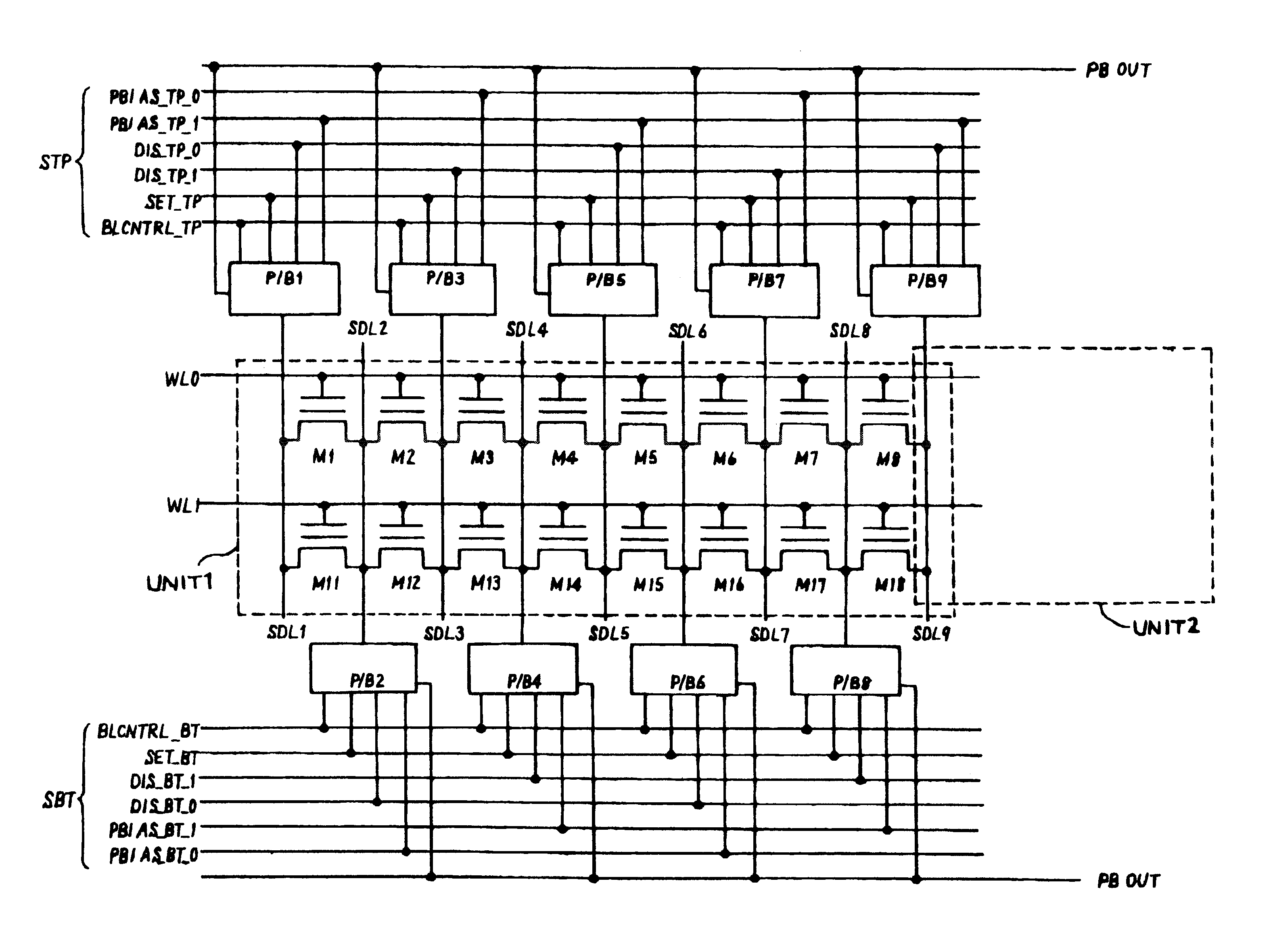
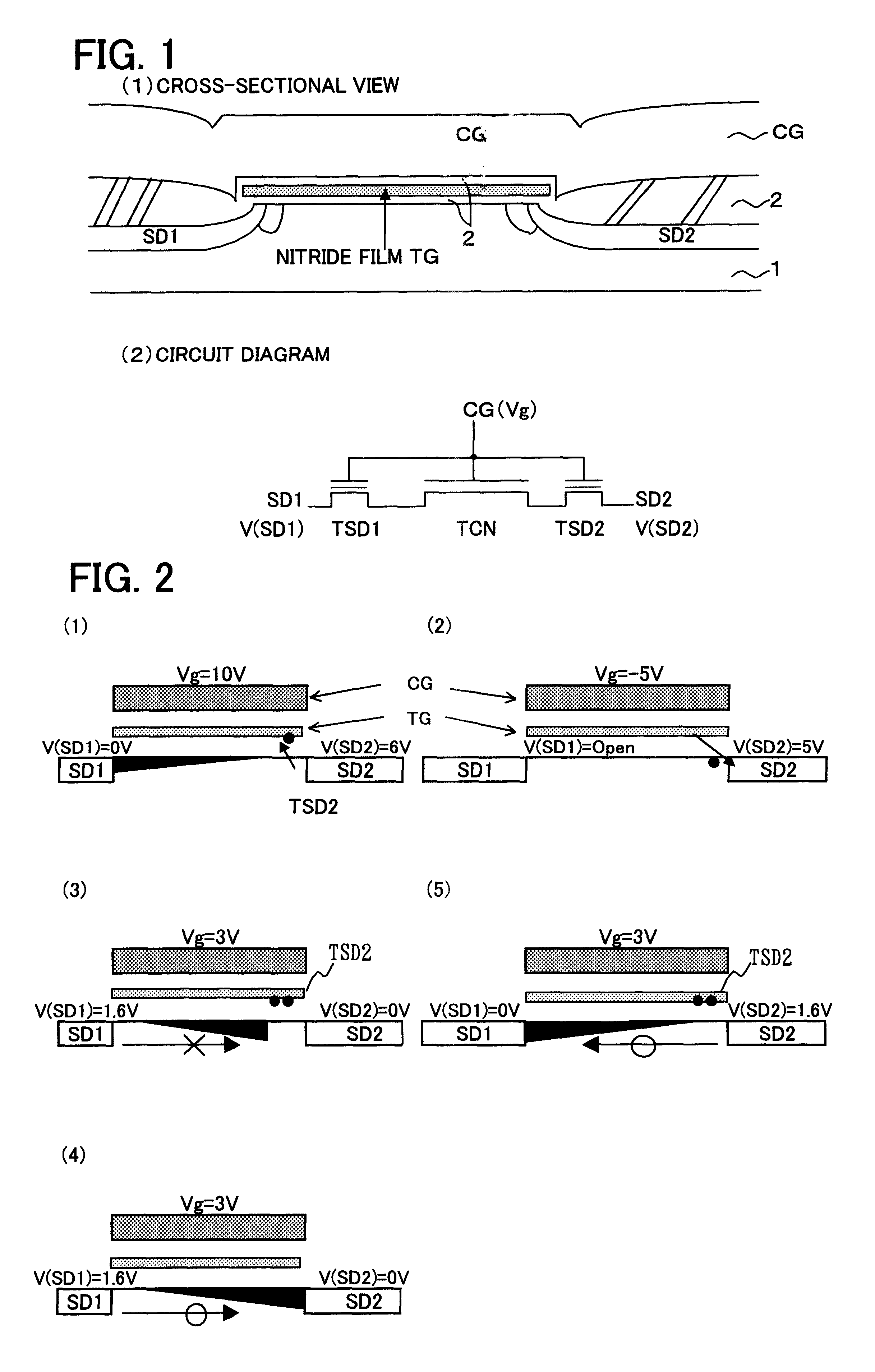
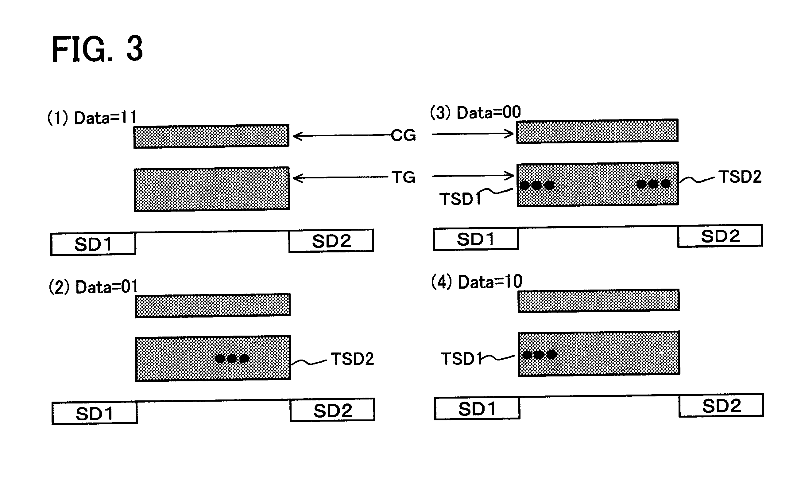
The embodiment of the present invention is a non-volatile memory circuit which has a plurality of cell transistors capable of storing two bits. Cell transistors of this kind are the same as the conventional cell transistors illustrated by FIGS. 1, 2, 3. In other words, two-bit information can be recorded in a single cell transistor according to whether or not electrons are trapped at both ends of a non-conductive trapping gate. For this reason, programming (write), erase and read-out operations with respect to a cell transistor are as shown in FIG. 2, and a repeat description thereof is not provided here.

FIG. 6 is a figure to show the cell array constitution of the present embodiment in which a plurality of such cell transistors are arranged in a matrix. In the cell array shown in FIG. 6, two word...


PUM


Abstract

The present invention provides a multi-bits non-volatile memory circuit having a cell transistor with non-conductive trap gate which has a cell array capable of reading a plural data simultaneously. The present invention is a non-volatile memory circuit in which a plurality of cell transistors M having a non-conductive trapping gate TG are arranged, comprising: a plurality of source-drain lines SDL, which are connected commonly with the source-drain regions SD1, SD2 of cell transistors adjacent in row direction, wherein these adjacent source-drain lines are set to a floating state F, a read-out voltage application state BL, a reference voltage state OV, a read-out voltage state BL, and a floating state F, and the source-drain lines SDL in the read-out voltage state is caused to function as bit lines, such that a plurality of data are read out simultaneously. The above states are generated by the page buffer P / B connected to the source-drain line. The data read and hold are performed by the page buffer.

Description

The present invention relates to a non-volatile memory circuit constituted by cell transistors which have a non-conductive trapping gate and which are capable of storing multiple bit data, and, more particularly, to a non-volatile memory circuit which has a cell array constitution capable of simultaneously reading out stored data from a multiplicity of cell transistors.TECHNICAL BACKGROUNDNon-volatile memories that utilize semiconductors are widely used as information recording media because such non-volatile memories are capable of holding information even if the power supply is OFF, and of high speed read-out. In recent years, non-volatile memories have been utilized in mobile information terminals, and utilized as recording media for digital cameras and for digital music in the form of MP3 data, for example.Non-volatile memories, such as the flash memories that are currently in widespread use, are constructed having, on a channel region between a source region and drain region, a...

Claims


Application Information

Patent Timeline
Patent Type & Authority Patents(United States)
IPC IPC(8): G11C16/04G11C16/06G11C16/26G11C11/56G11C16/02
CPCG11C11/5671G11C16/0475G11C16/0491G11C16/26G11C16/06
Inventor KAWAMURA, SHOICHI
Owner SPANSION INC
Why Eureka
Try Eureka