Method for forming a silicide layer of semiconductor device

a technology of semiconductor devices and silicide layers, which is applied in the manufacturing of semiconductor/solid-state devices, basic electric elements, electric devices, etc., can solve the problems of excessive junction leakage current, reduced junction interface actual width, and reduced junction leakage current of conventional silicide layers, so as to reduce junction leakage current and minimize the effect of electrical property deterioration

Inactive Publication Date: 2003-12-23
SK HYNIX INC
View PDF5 Cites 9 Cited by
  • Summary
  • Abstract
  • Description
  • Claims
  • Application Information

AI Technical Summary

Benefits of technology

Accordingly, a method for forming a silicide layer of a semiconductor device is disclosed wherein a shallow junction can be formed in a very small device, and which minimizes the deterioration of an electrical property of the semiconductor device by reducing junction leakage current, when the silicide layer is formed using Ti and Co as source materials.
A high rise speed of a temperature, a high drop speed of a temperature and a temperature are controlled through Spike RTA equipment so that an amorphous phase can be easily transformed to a crystalline phase. In addition, agglomeration with the implanted impurity is reduced due to deep reaction into the semiconductor substrate, and the time period during which the semiconductor substrate is maintained at a process temperature is controlled, thereby forming a complete crystalline silicide layer according to reaction between a metal Ti or Co and Si.
Moreover, a shallow junction can be formed and a junction leakage current property of the device can be improved by adjusting a physical distance between a silicide layer and Si diode junction interface in a source / drain region.

Problems solved by technology

As the semiconductor device is highly integrated, a parasitic resistance as well as a channel resistance existing below a gate increases in a degradation of the performance of the device.
Especially, CoSi.sub.2 which is more than 50% thicker than TiSi.sub.2, reduces a physical distance between the CoSi.sub.2 and Si diode junction interface in the source / drain region, which results in an excessive junction leakage current.
As described above, the conventional silicide layer decreases an actual width of the junction interface due to large consumption of the substrate.
In addition, excessive junction leakage current is generated thereby deteriorating the properties of the silicide layer.

Method used


Image

  • Method for forming a silicide layer of semiconductor device
  • Method for forming a silicide layer of semiconductor device
  • Method for forming a silicide layer of semiconductor device

Examples


Embodiment Construction

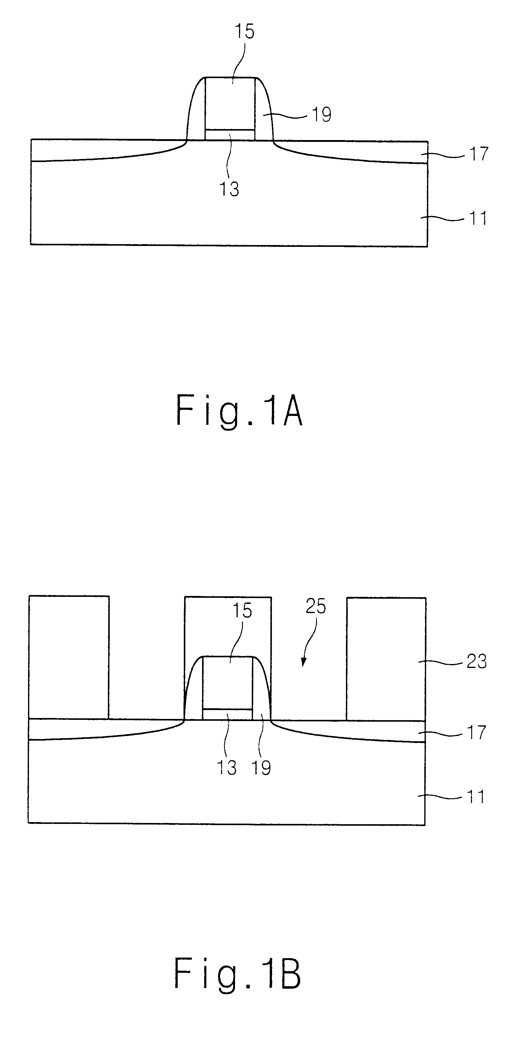
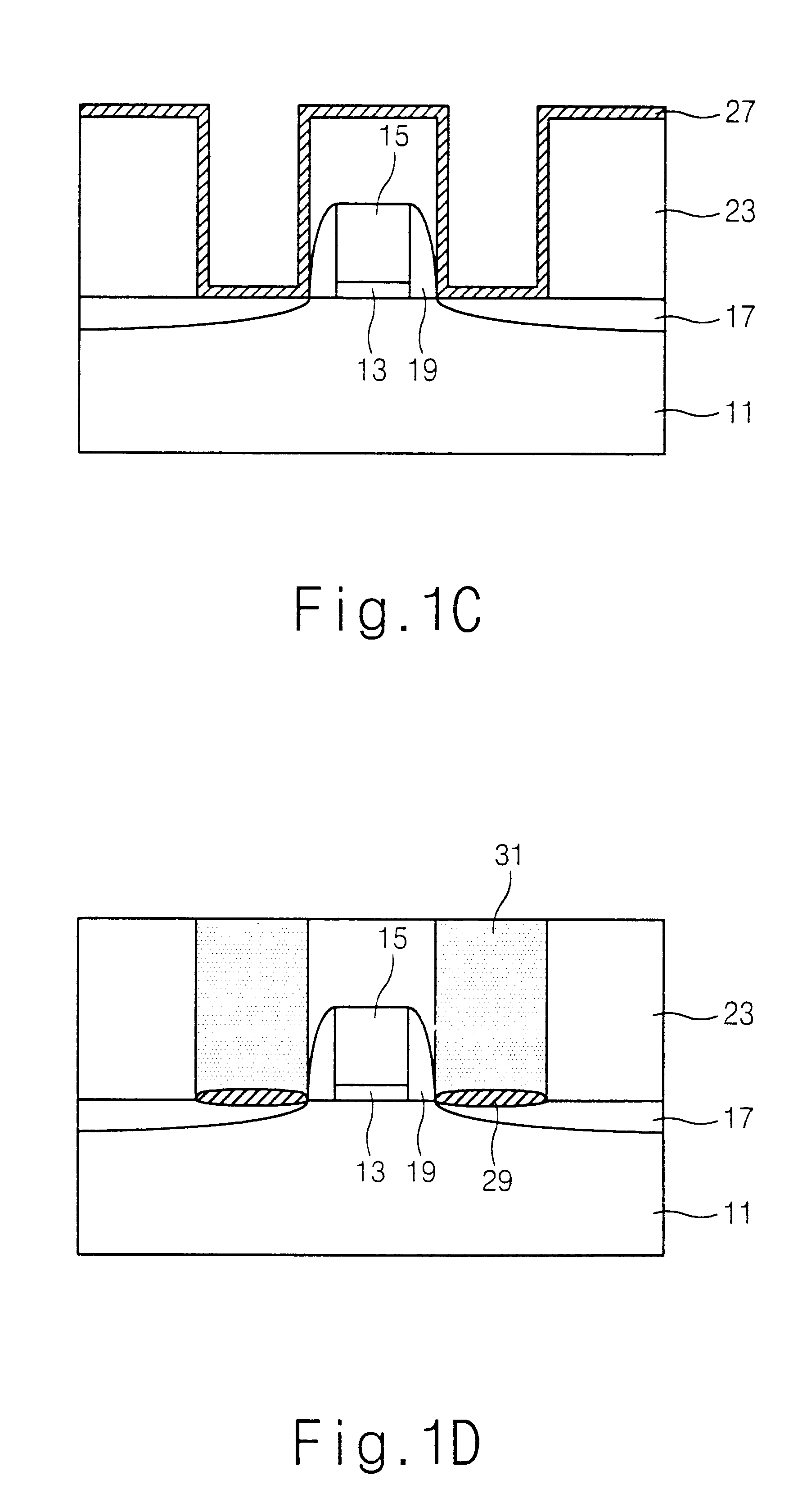
A method for forming a silicide layer of a semiconductor device in accordance with a preferred embodiment will now be described in detail with reference to the accompanying drawings.

FIGS. 1a to 1d are views illustrating sequential steps of the method for forming the silicide layer of the semiconductor device in accordance with a preferred embodiment.

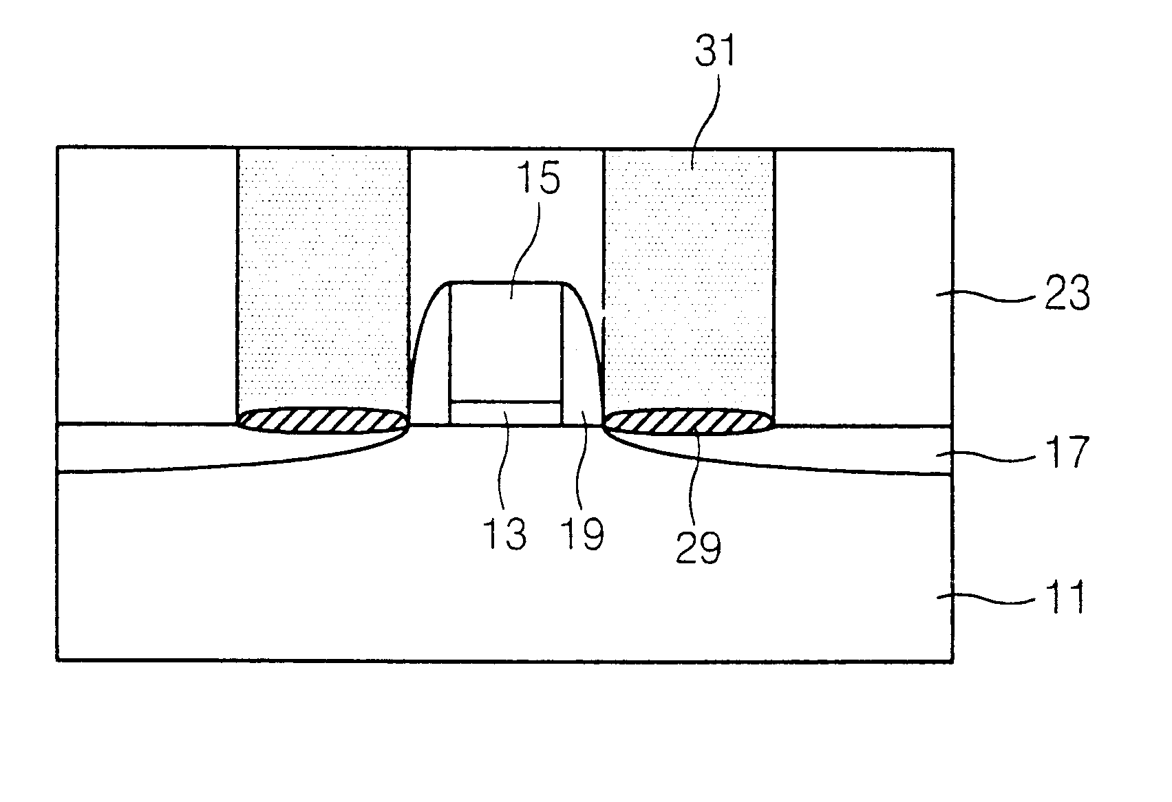
Referring to FIG. 1a, a gate electrode 15 is formed on a semiconductor substrate 11. Here, a gate oxide film 13 is positioned at the interface between the gate electrode 15 and the semiconductor substrate 11.

An insulating film spacer 19 is formed on the sidewall of the gate electrode 15, and an impurity junction region 17 is formed on the semiconductor substrate 11 using the gate electrode 15 and the insulating film spacer 19 as masks.

The impurity junction region 17 is an n-type or p-type depending on the type of the transistor, i.e. an NMOS or a PMOS in a CMOS. When the transistor is an n-type, the impurity junction region 17 is formed ...


PUM

PropertyMeasurementUnit
temperatureaaaaaaaaaa

Abstract

A method for forming a silicide layer of a semiconductor memory device is disclosed. A silicide layer is formed in an impurity junction region through a contact hole exposing the impurity junction region on a semiconductor substrate. Here, two thermal annealing processes are performed on the semiconductor substrate on which a metal layer is deposited, by using low and high temperature up speeds and maintaining the semiconductor substrate under the highest temperature for less than one second, and then dropping the temperature at high speed. The process for removing a portion of the metal layer which did not react is carried out. As a result, a shallow junction can be formed in a very small devices, and deterioration of an electrical property of the semiconductor device is minimized by reducing junction leakage current, which results in the rapid operation of the device.

Description

1. Technical FieldA method for forming a silicide layer of a semiconductor device is disclosed, and, in particular, in the disclosed method, the silicide layer has a low specific resistance and chemical stability and is positioned below a portion where a defective layer is formed, thereby improving at least one operational property of the resultant CMOS.2. Description of the Related ArtA silicide layer has a resistance 20 times lower than that of a source / drain region or a polysilicon gate. The silicide layer is essentially used in the CMOS. The silicide layer improves an operation speed which is one of the major factors which indicate an operational property of a semiconductor device.The silicide layer is formed by depositing a thin metal film on a semiconductor substrate and thermally treating the resulting structure. Since the silicide layer has a low specific resistance and chemical stability and is positioned below portion where a defective layer is formed, it is used in the mo...

Claims


Application Information

Patent Timeline
Patent Type & Authority Patents(United States)
IPC IPC(8): H01L21/285H01L21/02H01L21/336
CPCH01L21/28518H01L21/18
Inventor RYOO, CHANG WOOLEE, JEONG YOUBSOHN, YONG SUN
Owner SK HYNIX INC
Why Eureka
Try Eureka