Method of detecting pattern defects

a pattern and defect technology, applied in the field of pattern defect detection, can solve the problems of inability to detect minute defects, normal patterns may be detected as failures,

Inactive Publication Date: 2004-03-30
PANASONIC CORP
View PDF17 Cites 6 Cited by
  • Summary
  • Abstract
  • Description
  • Claims
  • Application Information

AI Technical Summary

Problems solved by technology

On the other hand, normal patterns may be detected as failures if they contravene the pattern rules.
With the comparison method, minute differences b

Method used


Image

  • Method of detecting pattern defects
  • Method of detecting pattern defects
  • Method of detecting pattern defects

Examples


Embodiment Construction

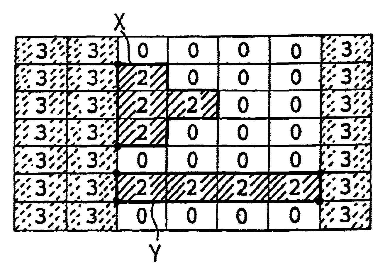
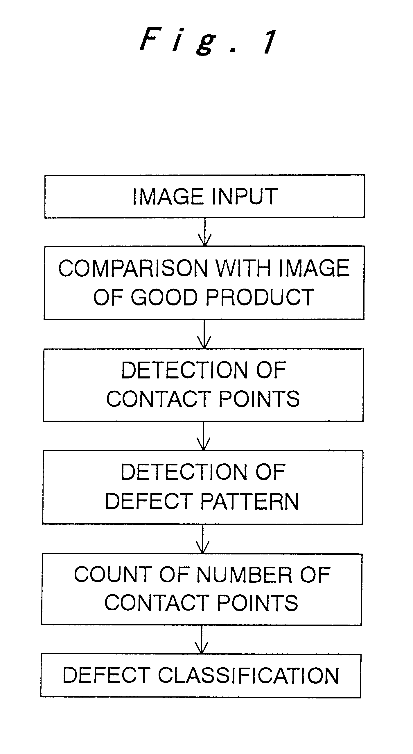
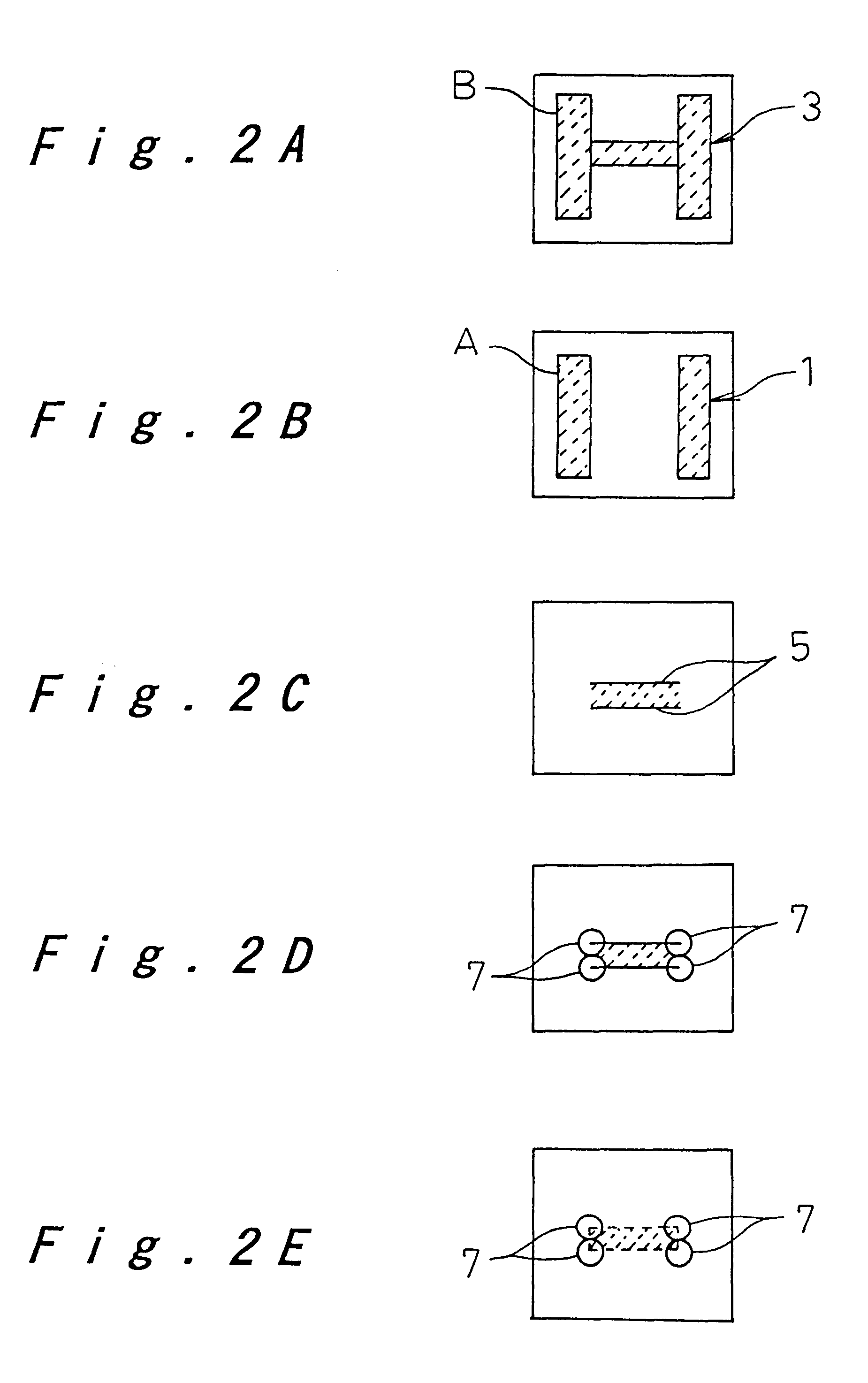
Preferred embodiments of a method of detecting pattern defects according to the present invention are described below with reference to FIG. 1 to FIG. 15.

FIG. 1 is a flow chart of a method of detecting pattern defects according to this embodiment. The method comprises: a step of inputting a subject pattern image; a step of comparing the subject pattern image with the image of a good product pattern that has been previously registered; a step of detecting outline points on the contour of one or other of the good product pattern and the subject pattern not overlapping with the other; a step of extracting contact points from the outline points, which are not in contact with two or more of the other outline points; a step of detecting as a defect pattern a continuous region where there is no mutual overlap between the subject pattern and the good product pattern; a step of counting the number of contact points contained in the defect pattern; and a step of classifying and detecting defe...


PUM


Abstract

An input subject pattern is compared with a good product pattern that is registered beforehand, and a different portion of these is detected as a defect pattern. The detected defect pattern is classified in accordance with the features of the contour of the defect pattern.

Description

1. Technical Field of the InventionIn the examination of patterns such as the wiring patterns of semiconductors, printed circuit boards, liquid crystals, or plasma display panels etc or printed / impressed patterns, the present invention relates to a method of detecting pattern defects whereby defects are classified and detected.2. Description of Related ArtConventional methods of detecting pattern defects include the design rule check (DRC) method and the comparison method. The DRC method involves detecting the pattern line width and pattern separation by image processing. If the detected line width or pattern separation as respectively shown in FIG. 16A and FIG. 16B is not in accordance with certain wiring or pattern rules, such is determined as a pattern defect. In the example shown in FIGS. 16A and 16B, the line width and the pattern separation are both smaller than predetermined values, and therefore are detected as failures. The comparison method involves comparing a subject ima...

Claims


Application Information

Patent Timeline
IPC IPC(8): G01B11/30G01N21/88G06K9/48G06K9/20G06T7/00G06K9/68G06K9/00H01L21/66G06T1/00
CPCG06T7/0006G06T7/001G06T2207/30141G06T2207/30148
Inventor WAKITANI, KOICHIYUKAWA, NORIAKI
Owner PANASONIC CORP
Why Eureka
Try Eureka