Clock regeneration circuit

a clock signal and circuit technology, applied in the direction of electrial characteristics varying frequency control, phase-modulated carrier system, synchronisation signal speed/phase control, etc., can solve the problem of inability to reproduce the clock signal used for signal demodulation

Inactive Publication Date: 2004-06-01
JVC KENWOOD CORP A CORP OF JAPAN
View PDF20 Cites 23 Cited by
  • Summary
  • Abstract
  • Description
  • Claims
  • Application Information

AI Technical Summary

Problems solved by technology

It is, therefore, impossible to reproduce a clock signal used for signal demodulation through synchronous detection, by ex

Method used


Image

  • Clock regeneration circuit
  • Clock regeneration circuit
  • Clock regeneration circuit

Examples


first embodiment

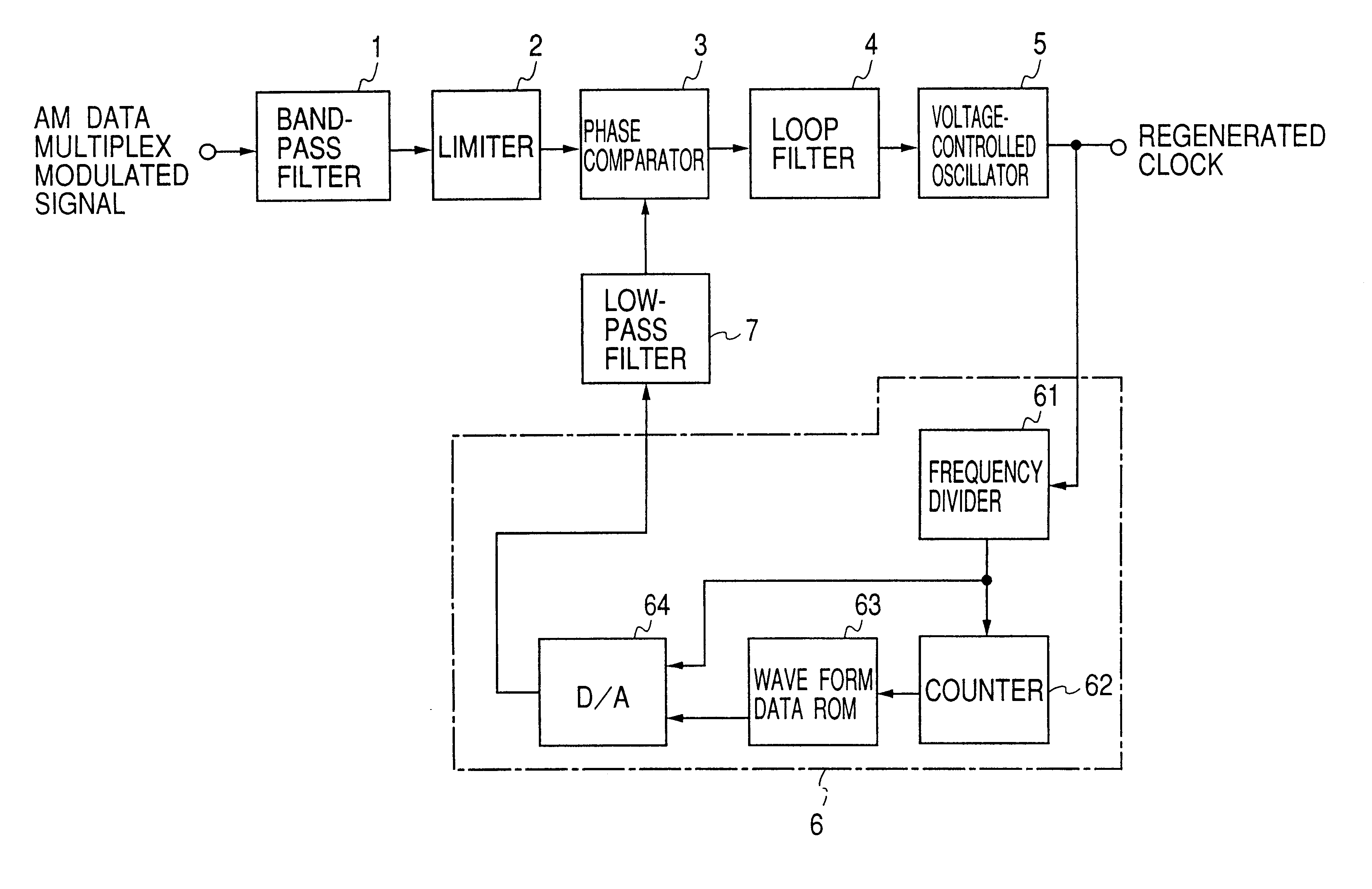
A clock regeneration circuit of this invention will be described with reference to preferred embodiments. FIG. 1 is a block diagram showing the structure of a clock regeneration circuit according to a first embodiment of the invention.

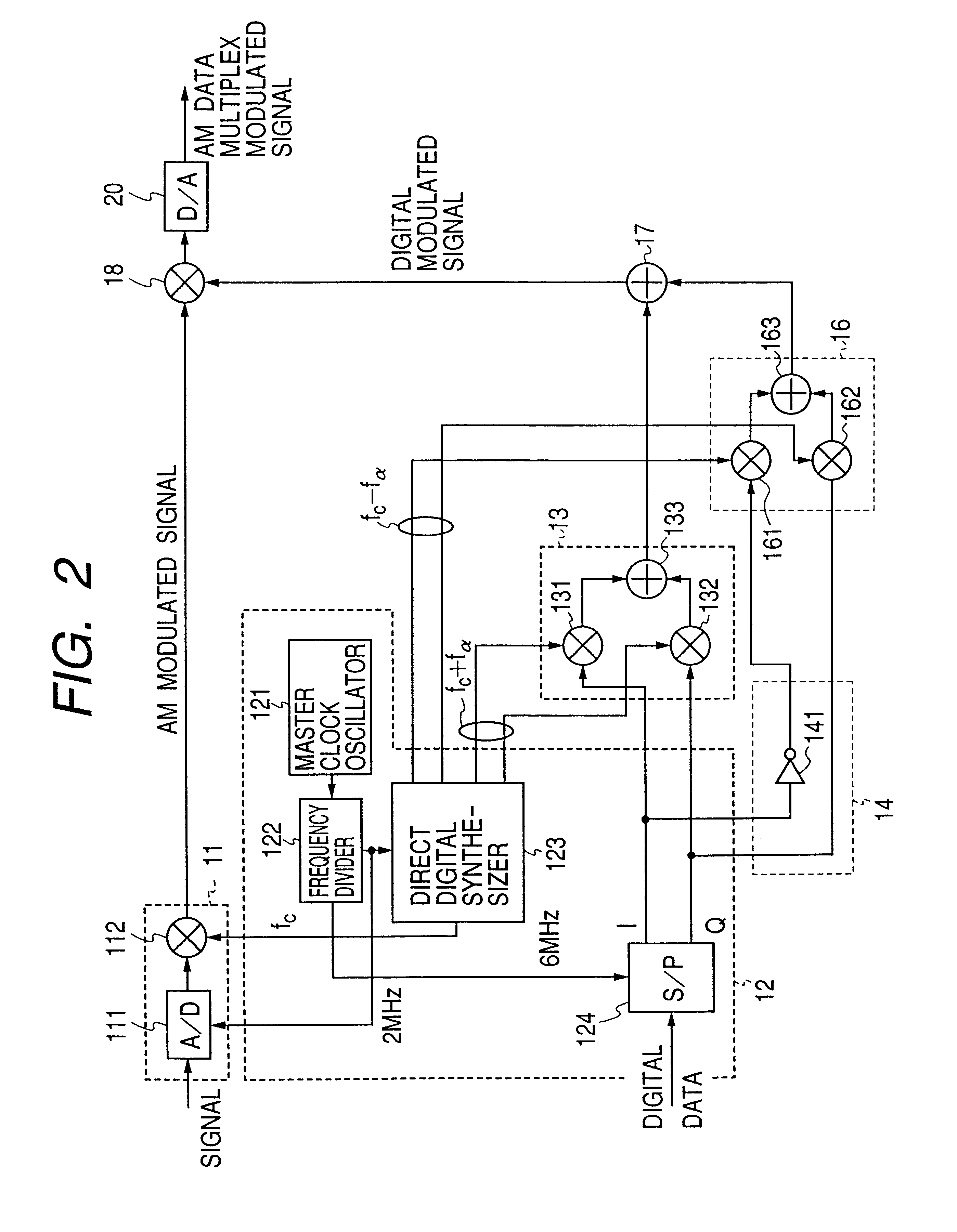
Prior to describing the clock regeneration circuit of the invention, an apparatus for generating an AM data multiplex modulated signal will be described with reference to FIG. 2.

In the AM data multiplex modulated signal generating apparatus, an analog signal (hereinafter simply called an input signal where applicable), such as a voice signal or the like is supplied to an AM modulator 11 in which the input signal is AM-modulated by a carrier having a frequency of fc generated by a frequency divider 122 to be later described. The AM modulator 11 is composed of an A / D converter 111 for A / D converting the input signal and a multiplier 112 for AM-modulating an output of the A / D converter 111.

The AM data multiplex modulated signal generating apparatus also i...

second embodiment

A clock regeneration circuit according to another embodiment of the invention is shown in FIG. 4. Referring to FIG. 4, an AM data multiplex modulated signal is supplied to a frequency converter 201 to be converted into an intermediate frequency. The AM data multiplex modulated signal converted into the intermediate frequency is band-limited by a band-pass filter 202 having a narrower band than the band width of the AM data multiplex modulated signal. The band-pass filter 202 extracts the carrier of the AM modulated signal from the AM data multiplex modulated signal.

The carrier extracted by the band-pass filter 202 is further supplied to a limiter 203 in which AM modulated components which are not removed by the band-pass filter 202 are removed. An output of the limiter 203 is supplied to a phase comparator 204. An output of the phase comparator 204 is supplied to a loop filter 205 composed of a low-pass filter to smooth the output of the phase comparator which is supplied to a volta...


PUM


Abstract

A clock regeneration circuit for regenerating a clock signal for demodulating data from an AM data multiplex modulated signal where digitally modulated signals are multiplexed in the same frequency band as those of an amplitude-modulated signal at the same time. The carrier for an amplitude-modulated signal is extracted from an AM data multiplex modulated signal where digitally modulated signals are multiplexed in the same frequency band as those of the amplitude-modulated signal at the same time through a band-pass filter, and the oscillation frequency of a voltage-controlled oscillator is controlled by the output of a phase comparator through a loop filter. The oscillation output of the voltage-controlled oscillator is supplied to a direct digital synthesizer and the phase of the carrier extracted through the band-pass filter is compared with the phase of the output of the direct digital synthesizer using the phase comparator. The oscillation output of the voltage-controlled oscillator is then synchronized with the carrier for the amplitude-modulated signal to produce a clock signal for demodulating data.

Description

The present invention relates to a clock regeneration circuit for regenerating a clock signal for data demodulation from an AM data multiplex demodulated signal which is obtained by multiplexing a digital modulated signal and an AM modulated signal in the same frequency band and at the same time.RELATED BACKGROUND ARTA conventional data multiplex method is roughly classified into a time division multiplex method used by character multiplex broadcasting of television broadcasting and a frequency multiplex method used by character multiplex broadcasting used by FM broadcasting. The frequency band occupied by AM broadcasting is narrow so that frequency multiplex and time division multiplex cannot be used. An AM data multiplex modulated signal generating apparatus for multiplexing an AM modulated signal and a digital modulated signal in the manner similar to data multiplex broadcasting in television or FM broadcasting, has not been realized as yet.The applicant of the present applicatio...

Claims


Application Information

Patent Timeline
IPC IPC(8): H04J9/00H03J7/02H04L27/22H03J7/06H04L7/04H04L7/06H04L27/06H03L7/18H03L7/16
CPCH04J9/00H04L7/06H04L27/066H03L7/1806
Inventor TADA, SHUNICHISHIRAISHI, KENICHI
Owner JVC KENWOOD CORP A CORP OF JAPAN
Why Eureka
Try Eureka