Method of fabricating a vertical quadruple conduction channel insulated gate transistor

a technology of conduction channel and gate, applied in transistors, electrical equipment, solid-state devices, etc., can solve the problems of limiting the effect of gate coupling phenomenon, without shortcomings, and no hope of producing very thin pillars

Inactive Publication Date: 2004-06-08
STMICROELECTRONICS SRL
View PDF9 Cites 33 Cited by
  • Summary
  • Abstract
  • Description
  • Claims
  • Application Information

AI Technical Summary

Problems solved by technology

Although these two approaches are useful, they are not without their shortcomings.
Thus at present there is no hope of producing very thin pillars (i.e. thinner than 50 nm) with conventional photolithography, which consequently limits the effectiveness of the gate coupling phenomenon.
For a relatively thick pillar, the junction depth can therefore be very large compared to the length of the channel, which is extremely unfavorable in terms of controlling the effects of short channels.

Method used


Image

  • Method of fabricating a vertical quadruple conduction channel insulated gate transistor
  • Method of fabricating a vertical quadruple conduction channel insulated gate transistor
  • Method of fabricating a vertical quadruple conduction channel insulated gate transistor

Examples


Embodiment Construction

It should be understood that these embodiments are only examples of the many advantageous uses of the innovative teachings herein. In general, statements made in the specification of the present application do not necessarily limit any of the various claimed inventions. Moreover, some statements may apply to some inventive features but not to others. In general, unless otherwise indicated, singular elements may be in the plural and vice versa with no loss of generality.

In the drawing like numerals refer to like parts through several views.

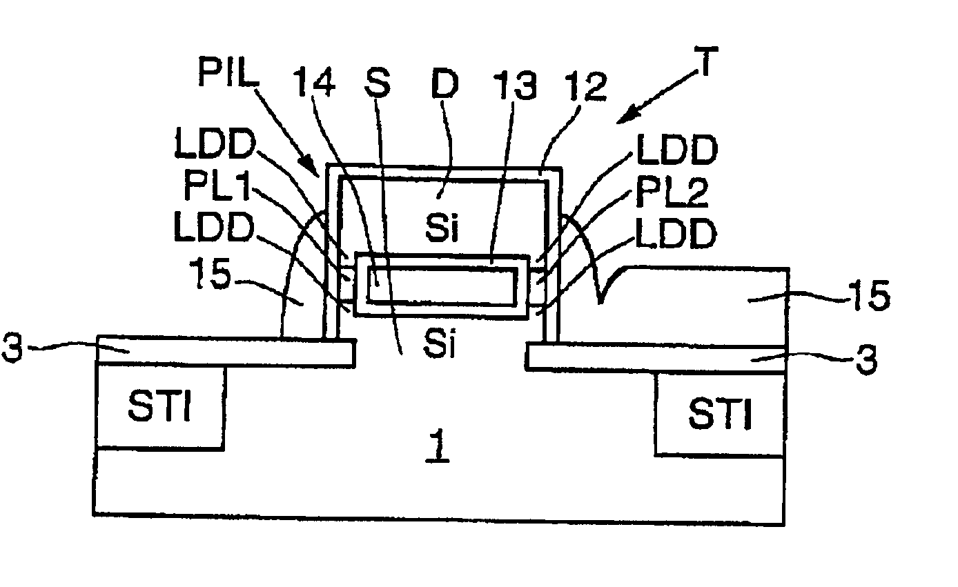
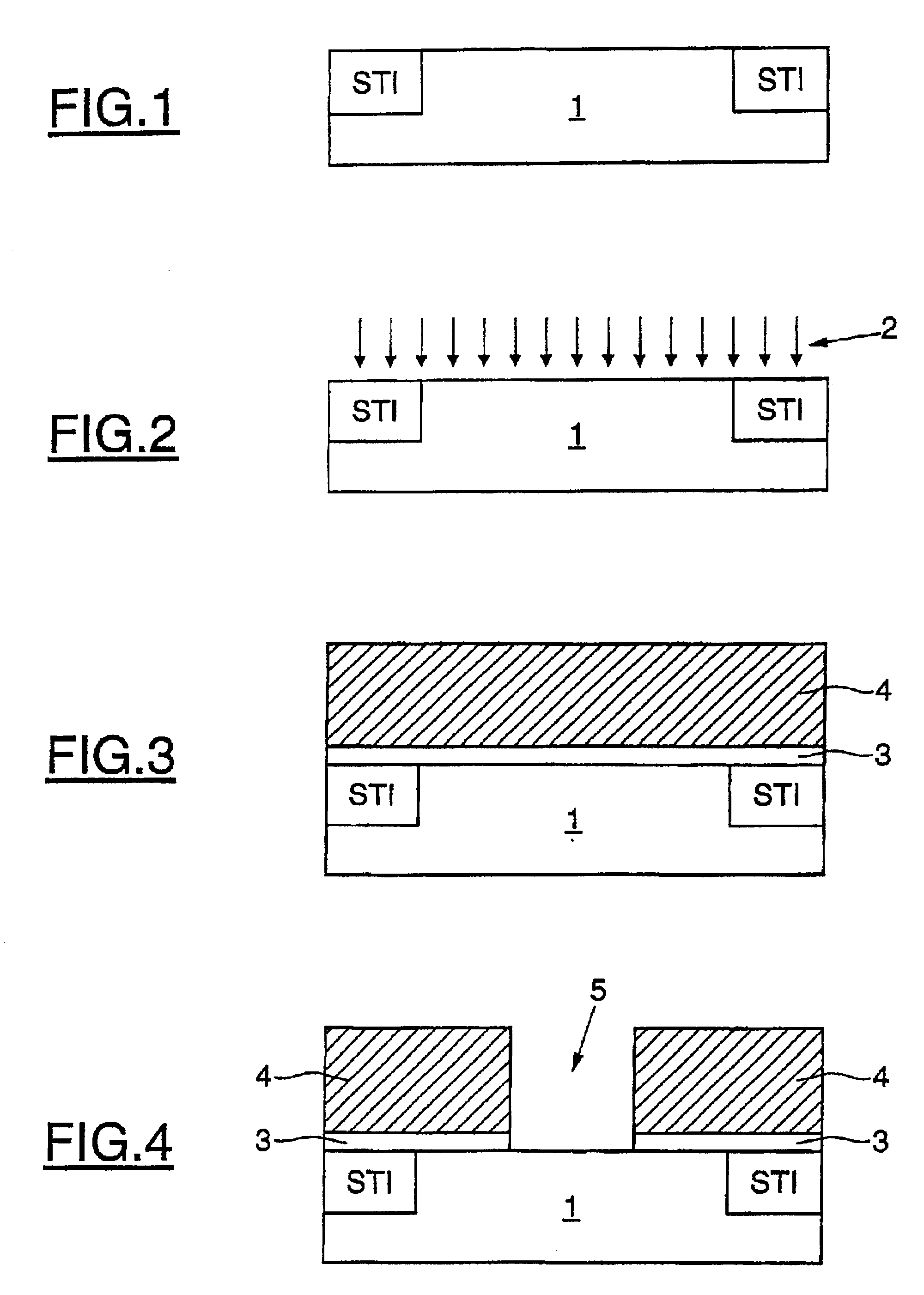
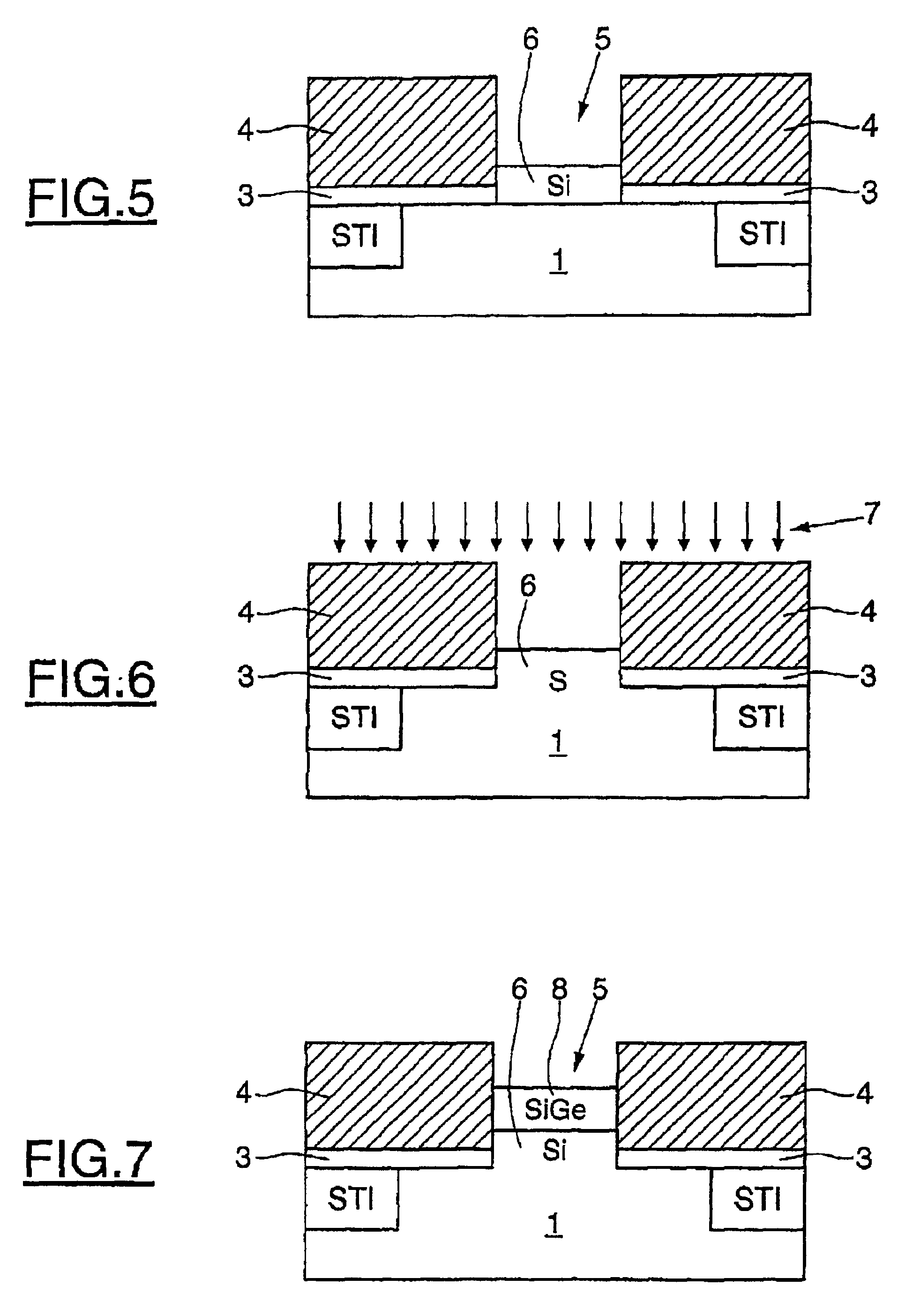
FIG. 1 shows a semiconductor, for example silicon, substrate 1 including lateral isolation areas STI using the shallow trench isolation technique. The lateral isolation areas STI delimit an active substrate area in and on which the future vertical transistor will be formed.

At this stage of the process, insulating wells are also implanted in the substrate 1. They are not shown in FIG. 1, for simplicity.

The substrate 1 is then implanted 2 (FIG. 2) wi...


PUM


Abstract

The vertical insulated gate transistor includes, on a semiconductor substrate, a vertical pillar incorporating one of the source and drain regions at the top, a gate dielectric layer situated on the flanks of the pillar and on the top surface of the substrate, and a semiconductor gate resting on the gate dielectric layer. The other of the source and drain regions is in the bottom part of the pillar PIL and the insulated gate includes an isolated external portion 15 resting on the flanks of the pillar and an isolated internal portion 14 situated inside the pillar between the source and drain regions. The isolated internal portion is separated laterally from the isolated external portion by two connecting semiconductor regions PL1, PL2 extending between the source and drain regions, and forming two very fine pillars.

Description

This application is based upon and claims priority from prior French Patent Application No. 0104437, filed Apr. 2, 2001, the disclosure of which is hereby incorporated by reference in its entirety.1. Field of the InventionThe present invention generally relates to the field of integrated circuits and more particularly to vertical insulated gate transistors.The invention applies in particular, although not exclusively, to high-speed logic circuits and radio-frequency circuits. More generally, the invention finds an application in technologies below 0.07 micron.2. Description of Related ArtThe vertical transistor is a device that overcomes the limitations of the planar MOS transistor, in lengths less than 0.1 micron. Its conduction body consists of a silicon pillar insulated and covered by a gate. It therefore has at least two conduction interfaces. Accordingly, the current I.sub.on and the transconductance per unit width are interfaces. Accordingly, the current I.sub.on and the trans...

Claims


Application Information

Patent Timeline
Patent Type & Authority Patents(United States)
IPC IPC(8): H01L21/336H01L21/02H01L29/78H01L29/66H01L29/02H01L29/165
CPCH01L29/66666H01L29/7827H01L29/165
Inventor SKOTNICKI, THOMASJOSSE, EMMANUEL
Owner STMICROELECTRONICS SRL
Why Eureka
Try Eureka