Method for electrochemical metallization and planarization of semiconductor substrates having features of different sizes

a technology of semiconductor substrates and features, applied in the direction of electrolytic processes, semiconductor devices, electrolysis components, etc., can solve the problem of difficult to achieve the complete filling of all features on a wafer

Inactive Publication Date: 2004-06-15
FARADAY TECH INC
View PDF6 Cites 77 Cited by
  • Summary
  • Abstract
  • Description
  • Claims
  • Application Information

AI Technical Summary

Benefits of technology

A further object is to provide a method for metallizing the surface of an etched semiconductor wafer without excessive overplate.

Problems solved by technology

However, it has been found that when the features, i.e., trenches, vias, and the like, formed on the surface of a semiconductor wafer are of different sizes, complete filling of all the features on a wafer is difficult to achieve, even when pulse reverse electroplating is used.

Method used


Image

  • Method for electrochemical metallization and planarization of semiconductor substrates having features of different sizes
  • Method for electrochemical metallization and planarization of semiconductor substrates having features of different sizes
  • Method for electrochemical metallization and planarization of semiconductor substrates having features of different sizes

Examples


example

An acid copper sulfate solution containing 60 g / L CuSO.sub.4, 9% by volume of H.sub.2 SO.sub.4, 60 ppm Cl.sup.-, and 350 ppm PEG was used as the copper electroplating bath for all experiments. The plating bath temperature was 25.degree. C. The plating experiments were conducted on 1.9.times.1.9 cm samples in a rotating electrode apparatus.

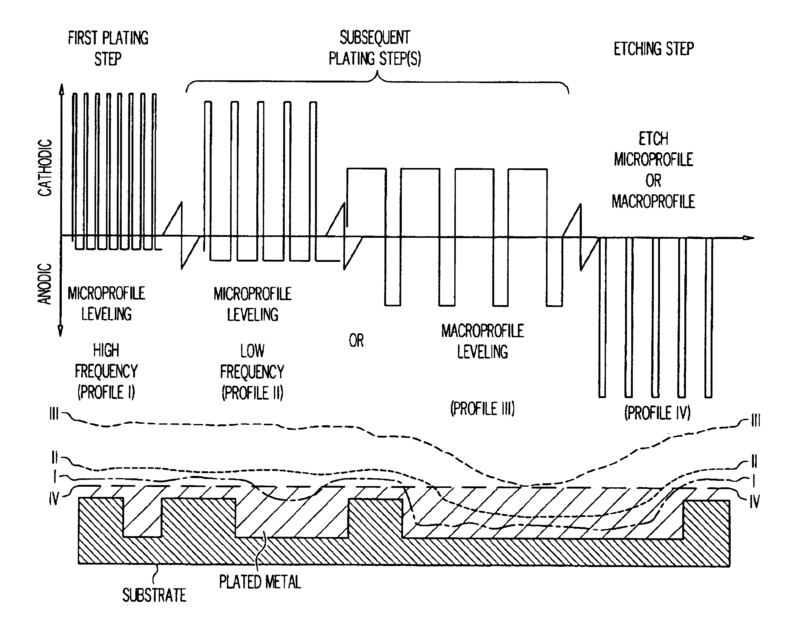
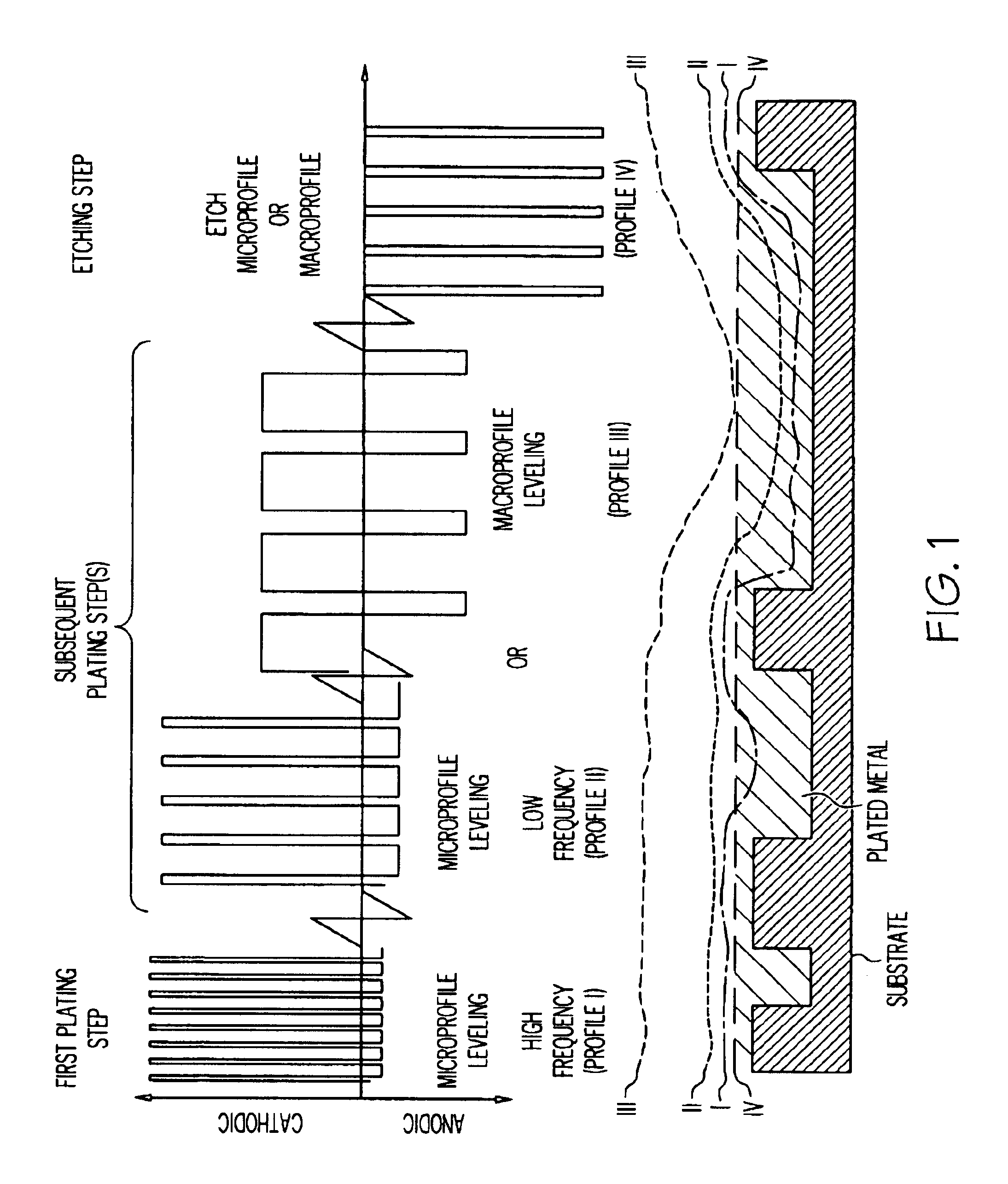
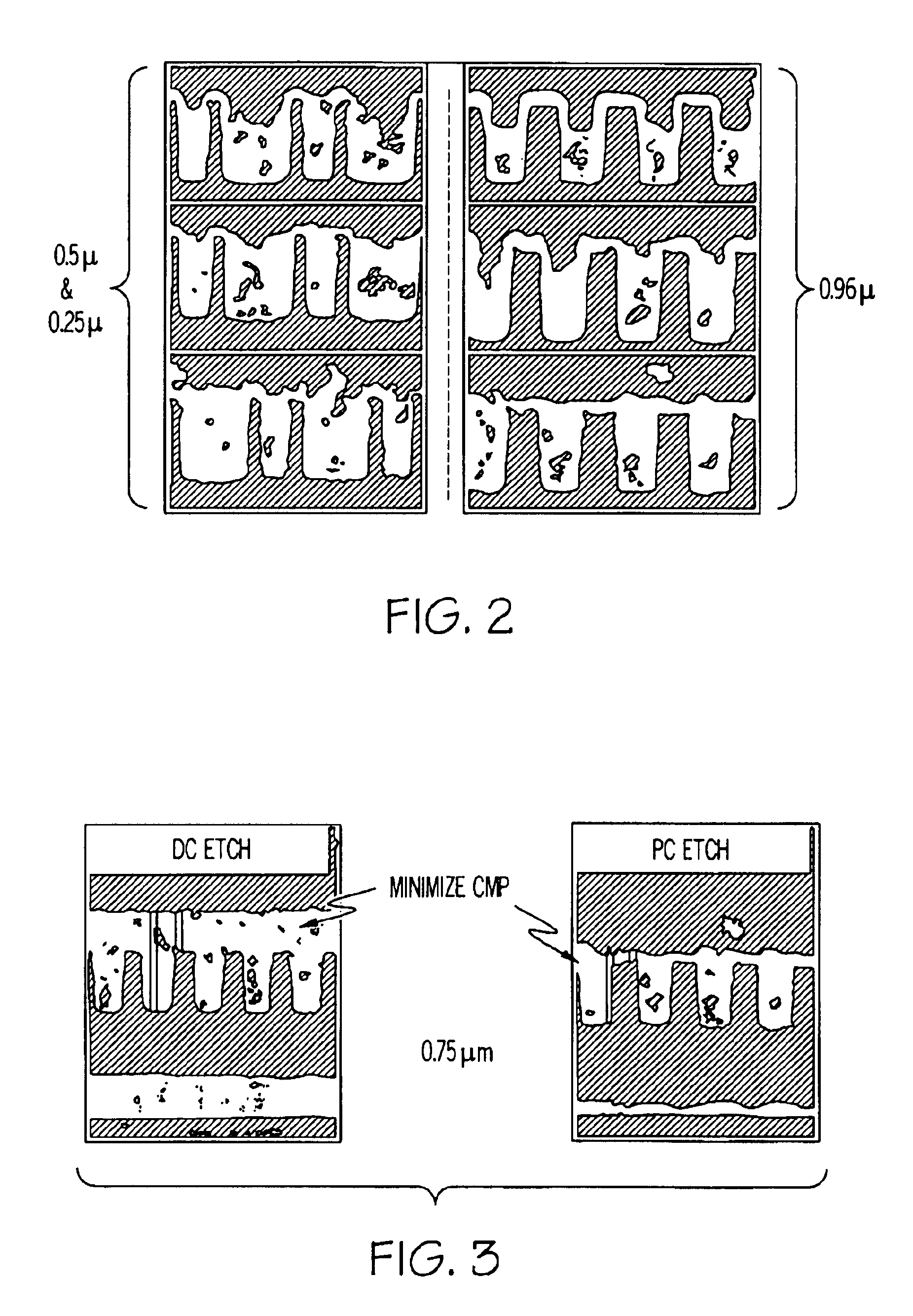
FIG. 2 shows metallization of VLSI features on IC's. Excellent, void-free filling for 0.25, 0.5, 0.75 and 1 .mu.m IC features were obtained with minimal overplate, using a waveform sequence consisting of a short forward on-time / long reverse on-time, followed by a short reverse on-time etching step. The reduction in the amount of chemical mechanical planarization (CMP) required in subsequent processing. FIG. 3 shows the reduction in overplate due to the use of electrically mediated pulsed current (PC) etching, as compared to DC etching.

Having described the invention in detail and by reference to particular embodiments thereof, it will be apparent th...


PUM

PropertyMeasurementUnit
on-timeaaaaaaaaaa
on-timeaaaaaaaaaa
diameteraaaaaaaaaa

Abstract

A method for filling recesses of different sizes on a semiconductor substrate comprising immersing a semiconductor substrate having a surface provided with recesses of different sizes in an electroplating bath containing ions of a metal to be deposited on the surface; immersing a counter electrode in the plating bath; passing an electric current between the substrate and the counterelectrode; wherein, in a first electroplating step, the electric current is a modulated reversing electric current comprising a train of pulses that are cathodic with respect to the substrate and pulses that are anodic with respect to the substrate, whereby the pulse train in the first step has a first period, the cathodic pulses have an on-time of from about 0.83 microseconds to about 50 milliseconds and the anodic pulses have an on-time of from about 42 microseconds to about 99 milliseconds, the cathodic and anodic pulses have a charge transfer ratio of the cathodic pulses to the anodic pulses that is greater than one; in a second electroplating step, the electric current is a, modulated reversing electric current comprising a train of pulses that are cathodic with respect to the substrate.

Description

1. Field of the InventionThis invention relates to metallization of semiconductor substrates and more particularly to metallization of semiconductor substrates having surface recesses of different sizes.2. Brief Description of the Prior ArtIn order to interconnect the transistors and associated devices on semiconductor wafers in the manufacture of integrated circuits, it is conventional to etch trenches, vias, and the like, into the surface of the silicon substrate, or into one or more layers of insulating material deposited thereon, and to deposit metal into these recessed structures. As the density of devices on the semiconductor chip has increased and the individual devices have become smaller, the connecting traces also have become smaller. In the manufacture of very large scale integrated (VLSI) chips and ultra large scale integrated (ULSI) chips, highly conductive metals, e.g., copper, have come to be used for the conductive traces, and attempts have been made to deposit the c...

Claims


Application Information

Patent Timeline
Patent Type & Authority Patents(United States)
IPC IPC(8): C25D5/18C25D5/00H01L21/70H01L21/288H01L21/02H01L21/768C25D7/12
CPCC25D5/18H01L21/2885H01L21/7684C25D5/02C25D7/12C25D5/627C25D5/611C25D7/123
Inventor TAYLOR, E. JENNINGS
Owner FARADAY TECH INC
Why Eureka
Try Eureka