Integrated circuit memory array with fast test mode utilizing multiple word line selection and method therefor

a technology of integrated circuit memory array and test mode, which is applied in the direction of information storage, static storage, digital storage, etc., can solve the problems of increased product manufacturing cost, difficult testing problems for manufacturers of integrated circuits that include write-once memory arrays (also known as one-time programmable, or otp memory arrays), and significant test time for each memory cell to perform a read mode tes

Inactive Publication Date: 2004-07-27
SANDISK TECH LLC
View PDF46 Cites 90 Cited by
  • Summary
  • Abstract
  • Description
  • Claims
  • Application Information

AI Technical Summary

Problems solved by technology

Manufacturers of integrated circuits that include write-once memory arrays (also known as one-time programmable, or OTP memory arrays), particularly those incorporating anti-fuse memory cells, face difficult testing problems.
One such problem concerns testing each unprogrammed memory cell, for it is desirable to test each memory cell to ensure that the unprogramm

Method used


Image

  • Integrated circuit memory array with fast test mode utilizing multiple word line selection and method therefor
  • Integrated circuit memory array with fast test mode utilizing multiple word line selection and method therefor
  • Integrated circuit memory array with fast test mode utilizing multiple word line selection and method therefor

Examples


Embodiment Construction

)

In the interest of clarity, not all of the routine features of the implementations described herein are shown and described. It will, of course, be appreciated that in the development of any such actual implementation, numerous implementation-specific decisions must be made in order to achieve the developer's specific goals, such as compliance with application- and business-related constraints, and that these specific goals will vary from one implementation to another and from one developer to another. Moreover, it will be appreciated that such a development effort might be complex and time-consuming, but would nevertheless be a routine undertaking of engineering for those of ordinary skill in the art having the benefit of this disclosure.

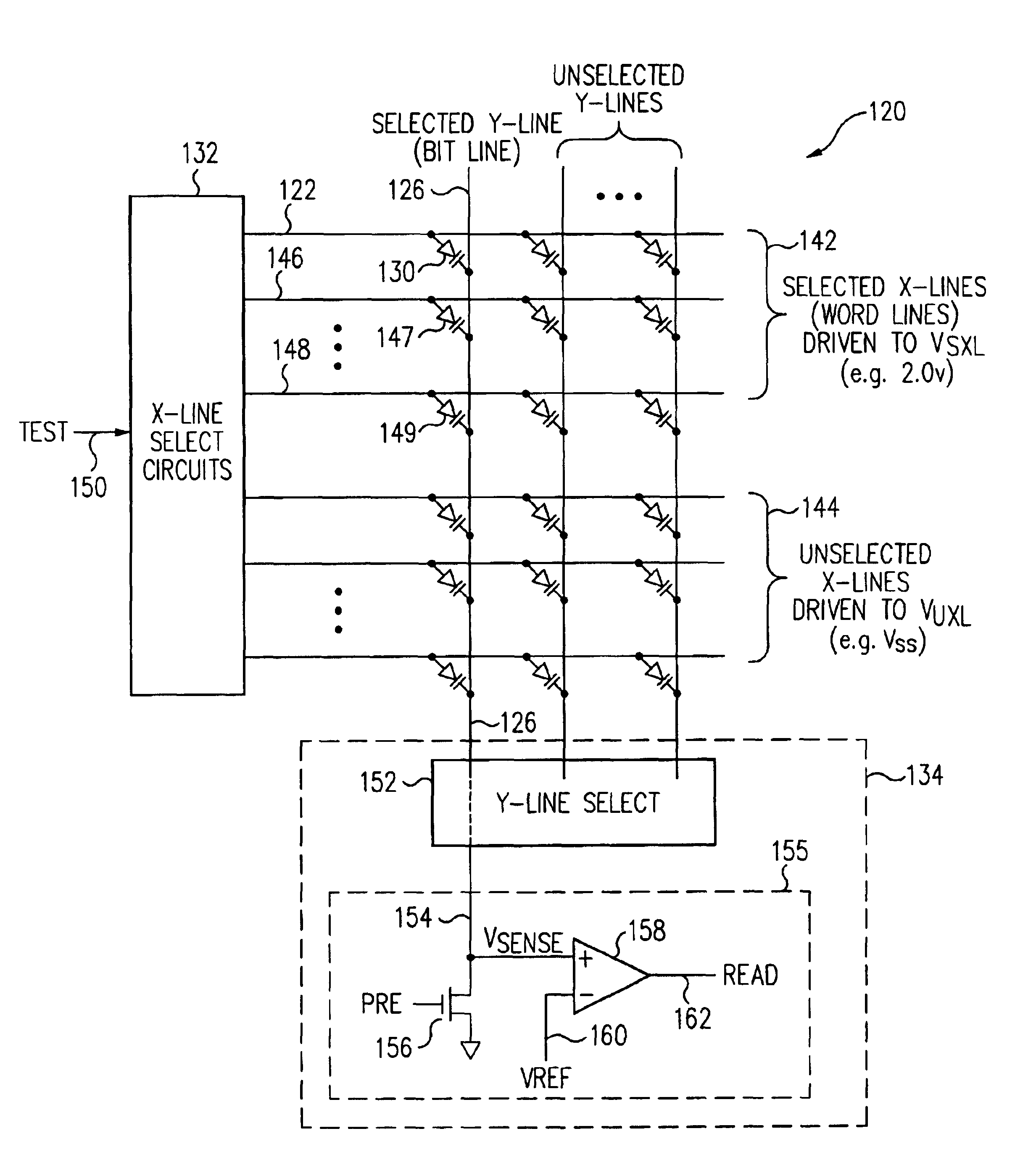
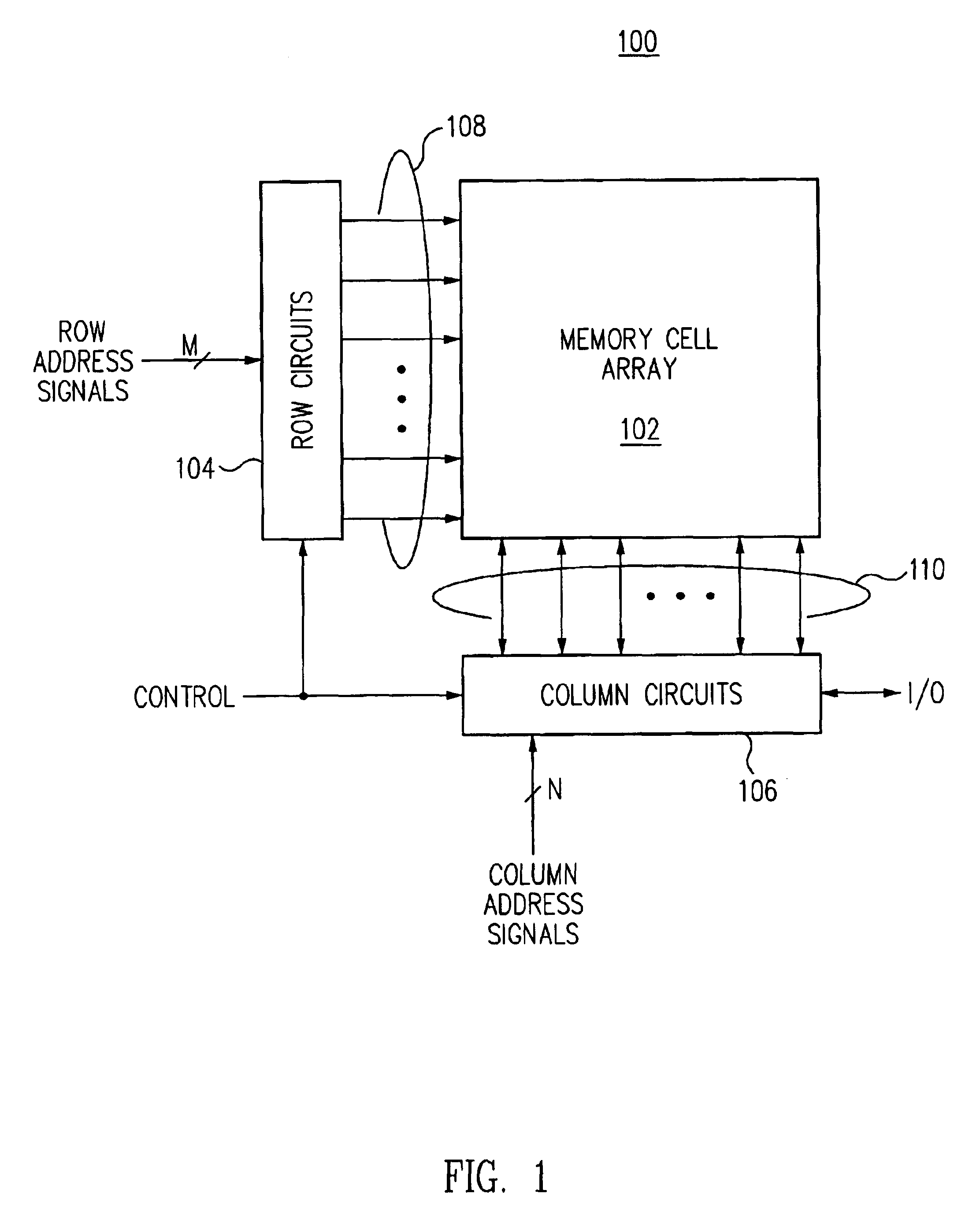
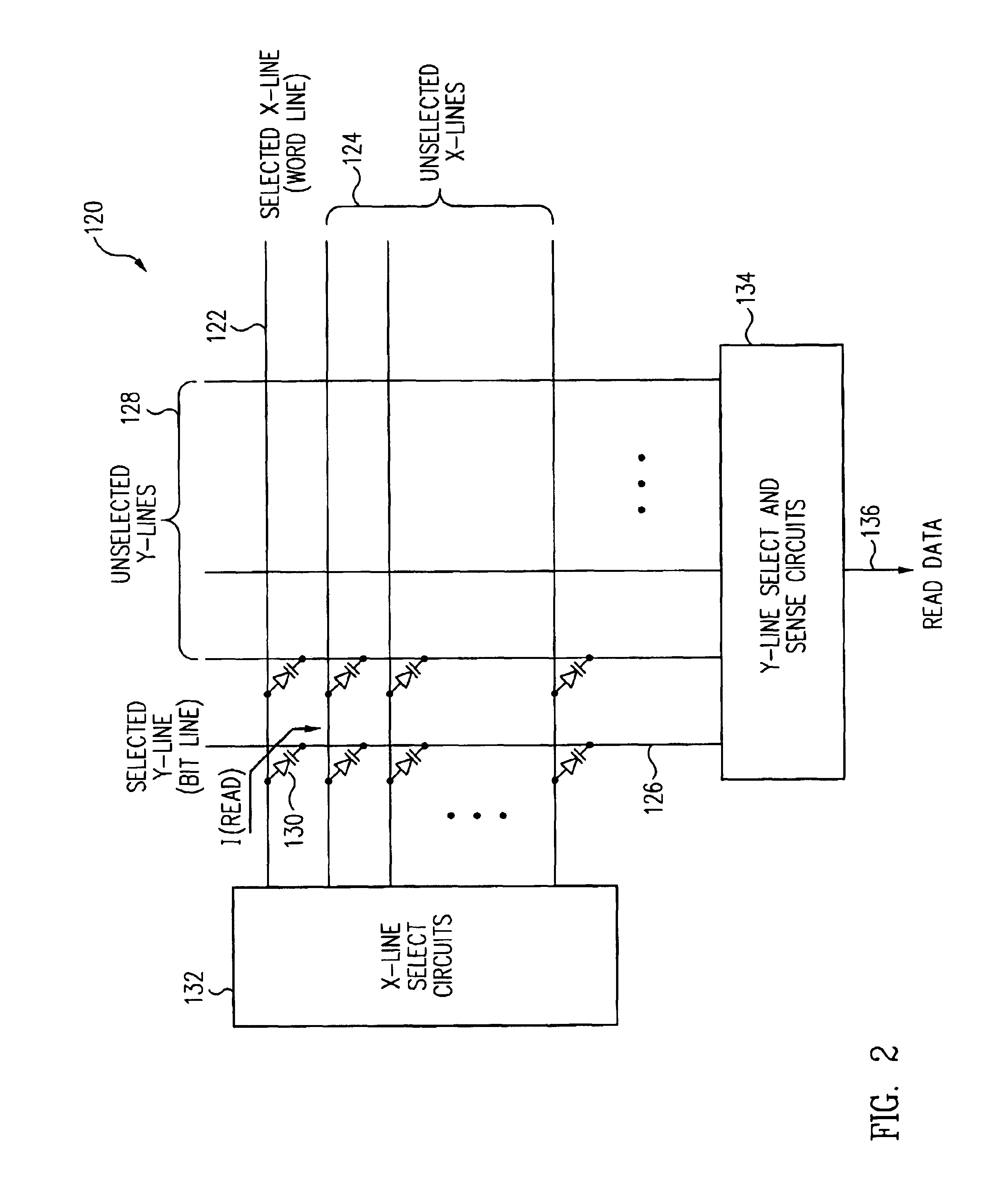
Referring now to FIG. 1, a block diagram is shown of an integrated circuit 100 including a memory array 102. In a preferred embodiment of the invention, the memory array 102 is preferably a three-dimensional, non-volatile, field-programmable write...


PUM


Abstract

In a programmable memory array, multiple memory cells on a single bit line may be tested in parallel for the unprogrammed state by simultaneously selecting multiple word lines associated with a selected bit line within a sub-array. A read current flowing through each selected memory cell is added on the selected bit line, and may be sensed using the same bit line sense circuits used for normal read operations. In the test mode, the sense circuit preferably indicates a pass/fail condition for all N simultaneously selected memory cells, which may be directly conveyed as an output signal, or may be combined with other similar pass/fail signals from other selected bit line sense circuits to generate a combined pass/fail output signal. Multiple bit lines may be simultaneously selected within the same sub-array. In addition, multiple sub-arrays may be simultaneously selected, each having one or more simultaneously selected bit lines, and the respective pass/fail signals conveyed directly or combined into fewer numbers of such signals.

Description

1. Field of the InventionThe present invention relates to semiconductor integrated circuit memory arrays, and particularly those incorporating write-once passive element memory cells incorporating anti-fuses.2. Description of the Related ArtManufacturers of integrated circuits that include write-once memory arrays (also known as one-time programmable, or OTP memory arrays), particularly those incorporating anti-fuse memory cells, face difficult testing problems. One such problem concerns testing each unprogrammed memory cell, for it is desirable to test each memory cell to ensure that the unprogrammed state (e.g., high-impedance state) exists at every memory cell location. A standard read mode test can be employed to ensure this. However, the test time required to perform such a read mode test of every memory cell is significant, especially in a very large array such as a three dimensional memory array having upwards of a billion memory cells. Such long test times contribute to incr...

Claims


Application Information

Patent Timeline
IPC IPC(8): G11C29/34G11C29/04
CPCG11C29/34G11C2029/1202G11C2029/2602
Inventor SCHEUERLEIN, ROY E.
Owner SANDISK TECH LLC
Why Eureka
Try Eureka