Variable flow deposition apparatus and method in semiconductor substrate processing

a technology of semiconductor substrates and flow deposition apparatus, which is applied in the field of vacuum processing chambers and methods for processing substrates, to achieve the effect of facilitating rapid opening and closing

Inactive Publication Date: 2004-08-17
APPLIED MATERIALS INC
View PDF20 Cites 120 Cited by
  • Summary
  • Abstract
  • Description
  • Claims
  • Application Information

AI Technical Summary

Benefits of technology

In one embodiment of the present inventions, an exhaust outlet in a vacuum processing chamber includes a nonsealing flow restrictor which can facilitate rapid opening and closing of the flow restrictor in some applications. Such a flow restrictor may be used in a variety of different chambers and deposition methods. It is believed that a nonsealing flow restrictor in accordance with the present invention is well suited to fast cycle deposition sequences such as atomic layer depositions (ALD).
Because the flow restrictor is a nonsealing flow restrictor, the conductance of the flow restrictor in the closed position may not be zero. However, the flow restrictor can restrict the flow of an exhaust gas from the chamber to permit the retention of sufficient processing gas in the chamber to deposit a film on the substrate or otherwise react with the substrate. In a preferred embodiment, the flow restrictor is a near sealing flow restrictor. After the desired film has been deposited or the processing of the substrate has been completed, the exhaust flow restrictor may be opened such that the flow restrictor conductance is significantly increased to a second, higher flow rate to facilitate exhausting residue gas from the chamber.

Problems solved by technology

However, the flow restrictor can restrict the flow of an exhaust gas from the chamber to permit the retention of sufficient processing gas in the chamber to deposit a film on the substrate or otherwise react with the substrate.

Method used


Image

  • Variable flow deposition apparatus and method in semiconductor substrate processing
  • Variable flow deposition apparatus and method in semiconductor substrate processing
  • Variable flow deposition apparatus and method in semiconductor substrate processing

Examples


Embodiment Construction

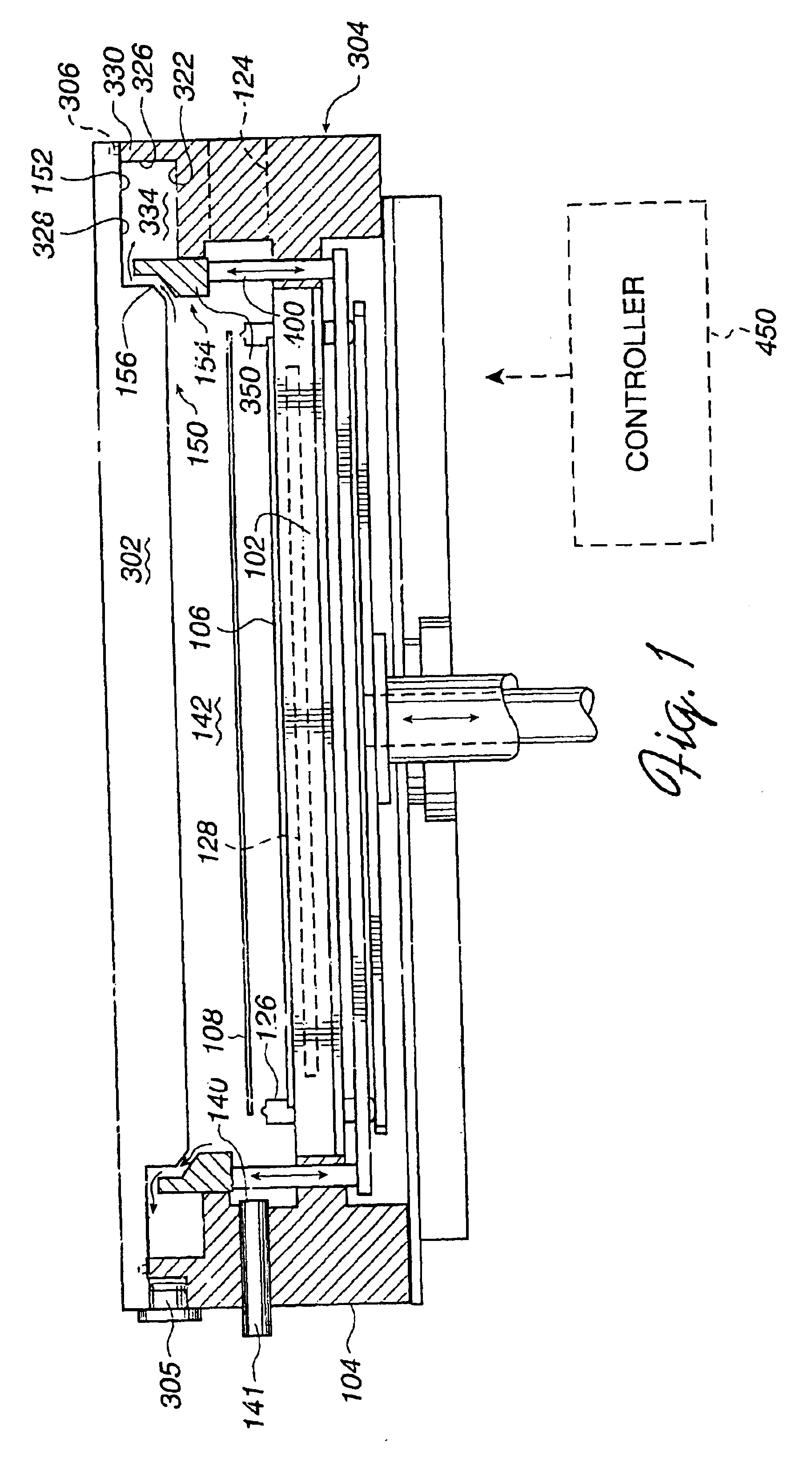
A processing chamber in accordance with a preferred embodiment of various aspects of the present inventions is indicated generally at 100 in FIG. 1. The processing chamber 100 includes a substrate support 102 having a support surface 106 which supports a substrate 108 in position for deposition of a layer of deposition material. The substrate 108 may be a silicon wafer, for example, or a glass substrate or other substrates upon which a layer of material may be deposited. Although the illustrative chamber 100 is depicted as a single substrate chamber, it is appreciated that the present inventions may be used in connection with multiple substrate chambers as well.

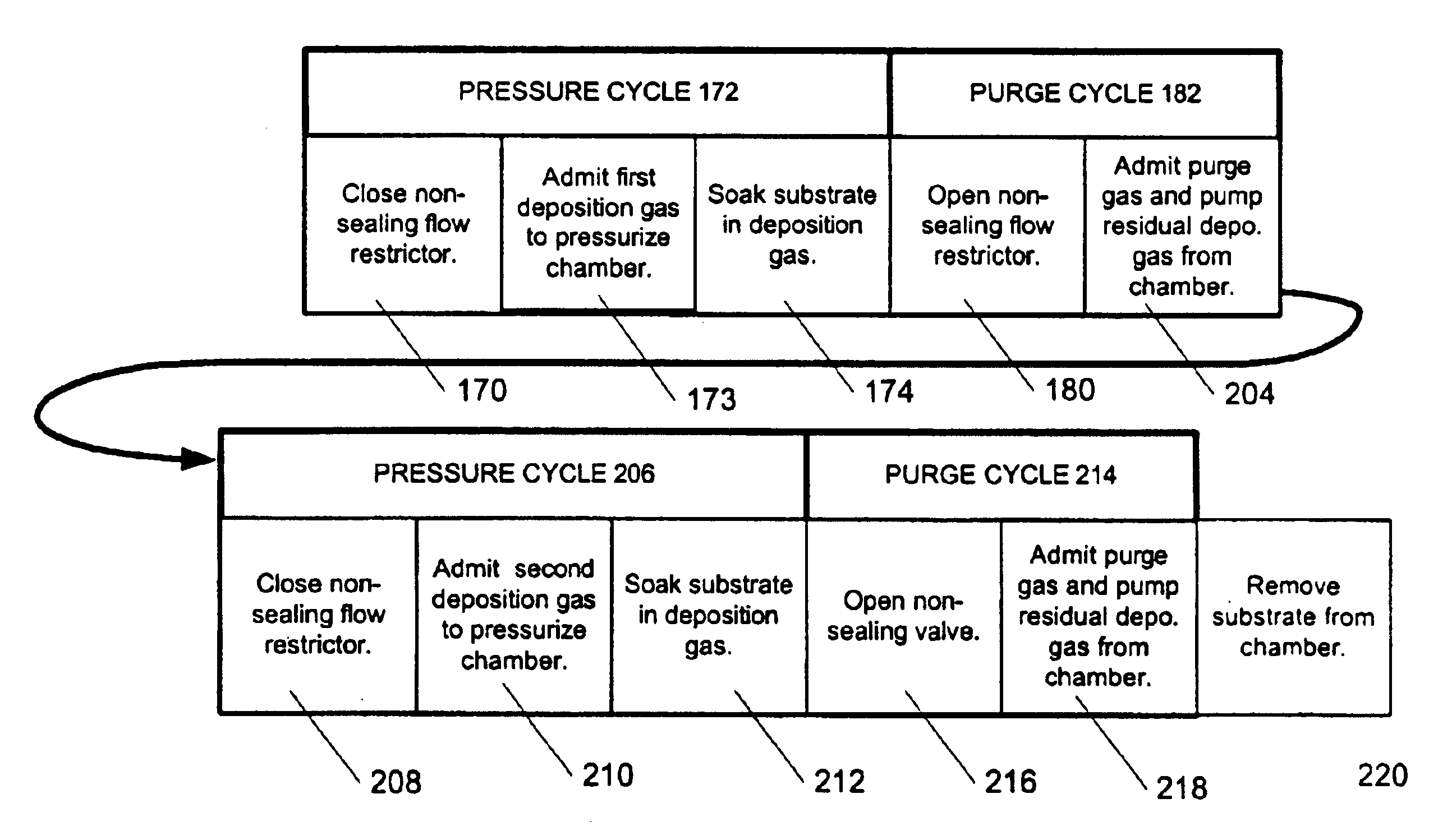
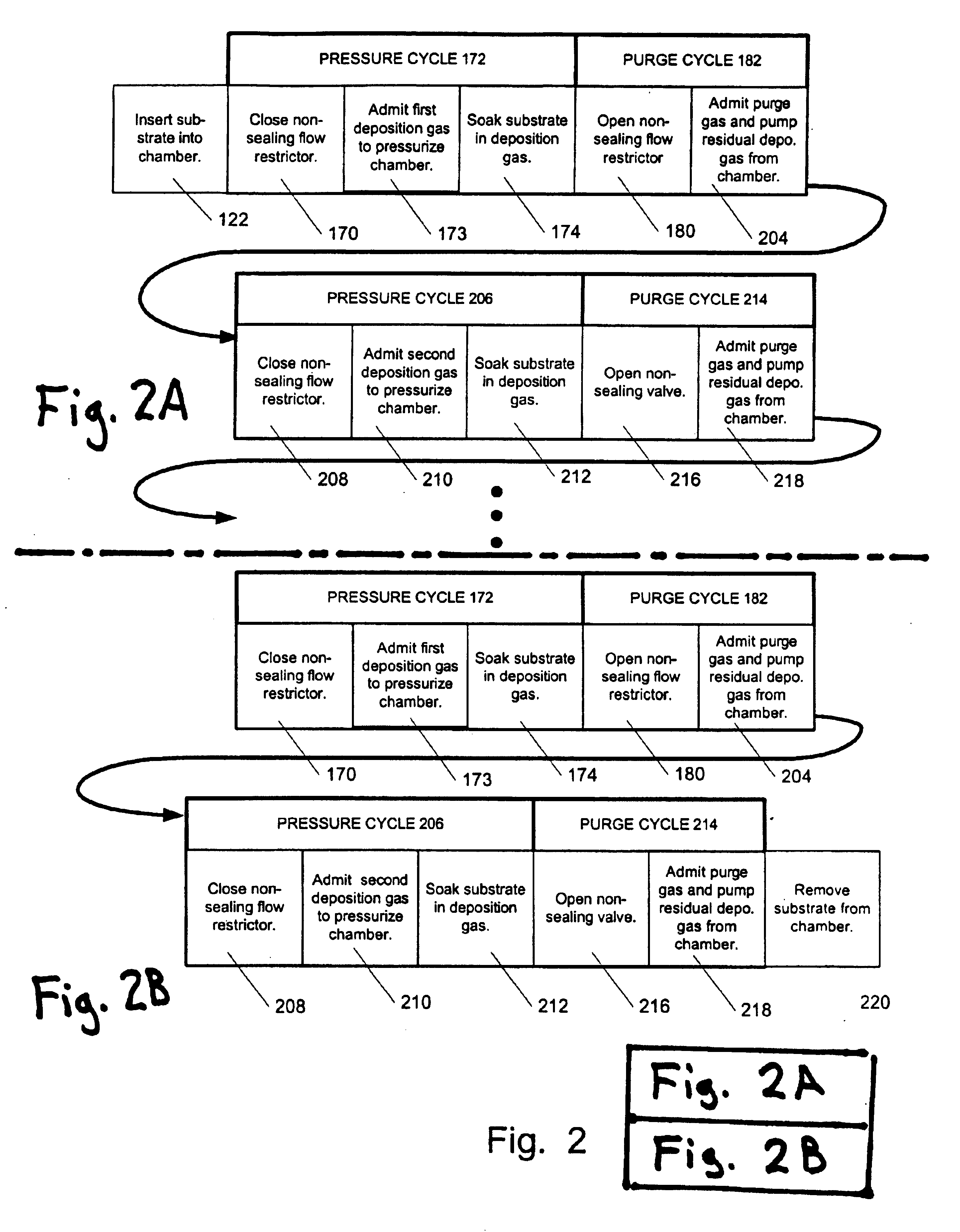
FIGS. 2A and 2B illustrate in schematic form a typical process 120 for depositing material on to a substrate such as the substrate 108 using the chamber 100. As explained in greater detail below, the present inventions have particular applicability to deposition processes such as atomic layer depositions in which many very th...


PUM

PropertyMeasurementUnit
thickaaaaaaaaaa
thickaaaaaaaaaa
pressureaaaaaaaaaa

Abstract

In one embodiment of the present inventions, an exhaust outlet in a vacuum processing chamber includes a nonsealing flow restrictor which can facilitate rapid opening and closing of the flow restrictor in some applications. Because the flow restrictor is a nonsealing flow restrictor, the conductance of the flow restrictor in the closed position may not be zero. However, the flow restrictor can restrict the flow of an exhaust gas from the chamber to permit the retention of sufficient processing gas in the chamber to deposit a film on the substrate or otherwise react with the substrate. After a film has been deposited, typically in a thin atomic layer, the exhaust flow restrictor may be opened such that the flow restrictor conductance is significantly increased to a second, higher flow rate to facilitate exhausting residue gas from the chamber. The nonsealing flow restrictor may be closed again to deposit a second layer, typically of a different material onto the substrate. The nonsealing flow restrictor may be rapidly opened and closed to deposit alternating layers of a variety of materials onto the substrate.

Description

FIELD OF THE INVENTIONSThese inventions relate to a novel vacuum processing chamber and method for processing substrates. More particularly, this invention relates to a vacuum processing chamber and processing method in which deposition gasses are admitted and exhausted from the chamber.BACKGROUND OF THE INVENTIONSSingle substrate processing chambers for substrates such as silicon wafers, have been used for some time because among other reasons, the chamber volume can be minimized, contamination of the substrate can be reduced, and the process control increased such that yields can be improved. Further, vacuum systems have been developed, such as described in Maydan et al, U.S. Pat. No. 4,951,601, that allow several sequential processing steps to be carried out in a plurality of vacuum processing chambers connected to a central transfer chamber, so that several processing steps can be performed on a substrate without its leaving a vacuum environment. This can further reduce contamin...

Claims


Application Information

Patent Timeline
Patent Type & Authority Patents(United States)
IPC IPC(8): C23C16/44H01L21/285H01L21/02C23C16/455
CPCC23C16/4412C23C16/45527H01L21/28562
Inventor TEPMAN, AVILEI, LAWRENCE CHUNG-LAI
Owner APPLIED MATERIALS INC
Why Eureka
Try Eureka