PCB component placement and trace routing therebetween
- Summary
- Abstract
- Description
- Claims
- Application Information
AI Technical Summary
Problems solved by technology
Method used
Image

Examples
Embodiment Construction
Preferred features of selected embodiments of this invention will now be described with reference to the figures. It will be appreciated that the spirit and scope of the invention is not limited to the embodiments selected for illustration. Also, it should be noted that the drawings are not rendered to any particular scale or proportion. It is contemplated that any of the configurations and materials described hereafter can be modified within the scope of this Invention.
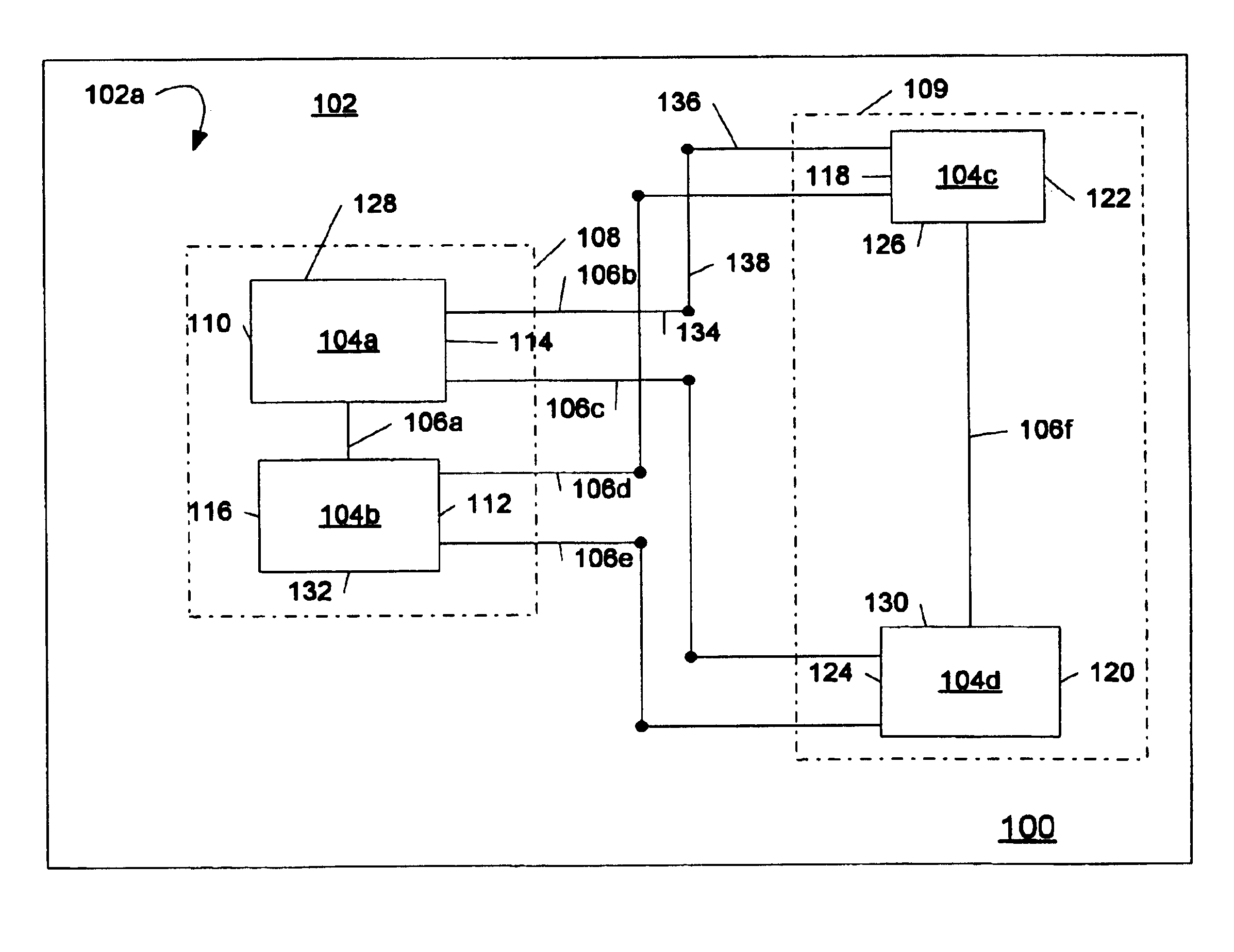
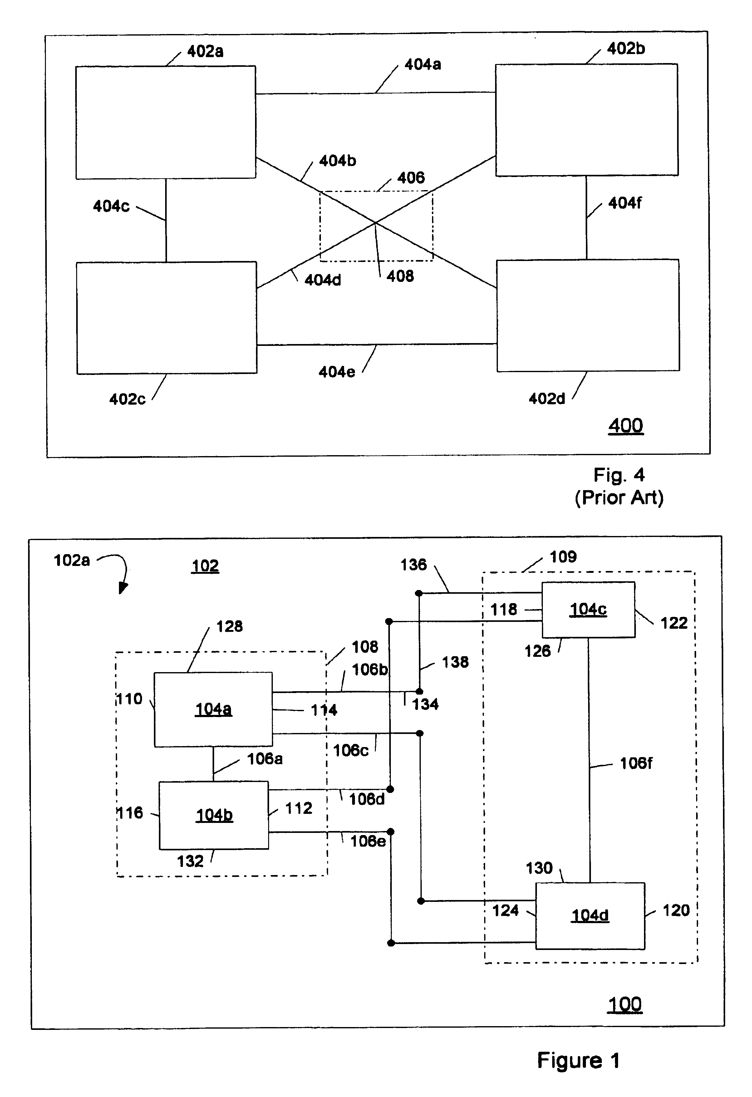
Referring to the figures generally, an exemplary printed circuit board 100 is provided. The printed circuit board 100 includes two pairs of electrical component-receiving footprints 108, 109 spaced from one another in a first direction (e.g., along the X axis) and a plurality of traces 106a-f interconnecting each of the footprints 104a-d. The footprints 104a-d in each of the pairs 108, 109 are substantially aligned in a second direction (e.g., vertically) substantially perpendicular to the first direction and at leas...
PUM
 Abstract
Description
Claims
Application Information