Semiconductor device and method for manufacturing the same

a semiconductor and semiconductor technology, applied in non-linear optics, instruments, optics, etc., can solve the problems of reducing the contrast of image display, the difficulty of simultaneously satisfying the improvement of opening ratio and the increase of pixels, and the number of contacts, so as to reduce the number of levels, improve the opening ratio, and reduce the number of contacts

Inactive Publication Date: 2004-12-07
SEMICON ENERGY LAB CO LTD
View PDF14 Cites 43 Cited by
  • Summary
  • Abstract
  • Description
  • Claims
  • Application Information

AI Technical Summary

Benefits of technology

Meanwhile, by forming a gate electrode and source and drain interconnections in the same process, it is possible to reduce the number of levels as compared to that of the conventional. Due to this, the physical distance is decreased between the semiconductor film and the light-shielding film, thus making possible to prevent against the occurrence of current leakage due to light leak or diffraction.
Meanwhile, the direct connection between the source interconnection and the source region makes it possible to reduce the number of contacts and improve the opening ratio. Amid continuing pixel size reduction, it is very effective to reduce the number of contact holes to a possible extent in order for improving the opening ratio.
Meanwhile, by forming holding capacitances by the drain interconnection, the first insulating film and the upper light-shielding film as well as the upper light-shielding film, the second insulating film and the pixel electrode, a sufficient holding capacitance can be secured. The holding capacitance can be further made sufficient by making the first and second insulating films to films having a high dielectric constant or in a possibly small thickness.
In this manner, by forming a gate electrode and source and drain interconnections in the same process, it is possible to reduce the number of levels as compared to that of the conventional. Thus, yield is improved and semiconductor-device manufacturing cost is reduced. Meanwhile, because the number of levels can be decreased, the physical distance is decreased between the semiconductor film and the light-shielding film, thus making possible to prevent against the occurrence of current leakage due to light leak or diffraction. Furthermore, the direct connection between the source interconnection and the source region makes it possible to reduce the number of contacts and improve the opening ratio. Meanwhile, sufficient holding capacitance can be secured by forming holding capacitances by the drain interconnection, the interlayer insulating film and upper light-shielding film as well as the upper light-shielding film, the first insulating film and the pixel electrode.

Problems solved by technology

Because the capacitor gradually decreases in its capacitance due to current leakage, it forms a cause to vary the amount of light transmission and hence decrease the contrast in image display.
The number of contacts is of a significantly important problem amid the continuing pixel size reduction.
However, amid continuing pixel size reduction, there is an extremely difficult problem in simultaneously satisfying the improvement in opening ratio and the increase in the number of pixels while designing a pixel structure with a sufficient capacitance secured.
When trying to realize such a pixel structure, the number of processes naturally increases to make the process complicate.
This results in a problem of worsened yield and semiconductor-device manufacture cost increase.
Meanwhile, there are cases that light leak current increases due to the light coming at a surface of a substrate not formed with TFTs of a light-transmission liquid crystal display or the light incident upon a top surface and irregularly reflected in the substrate, thus increasing an off-current (drain current flowing in a TFT off-state).
The increase in leak current requires an increase of holding capacitance for compensation, causing a problem of lowering in opening ratio in the pixel region.
Meanwhile, it is a problem to realize high-definition image display even in a liquid crystal display device designed with a pixel size as small as ten and several .mu.m square and in an electronic apparatus using, in a display part, such liquid-crystal display device.

Method used


Image

  • Semiconductor device and method for manufacturing the same
  • Semiconductor device and method for manufacturing the same
  • Semiconductor device and method for manufacturing the same

Examples


embodiments

Embodiment 1

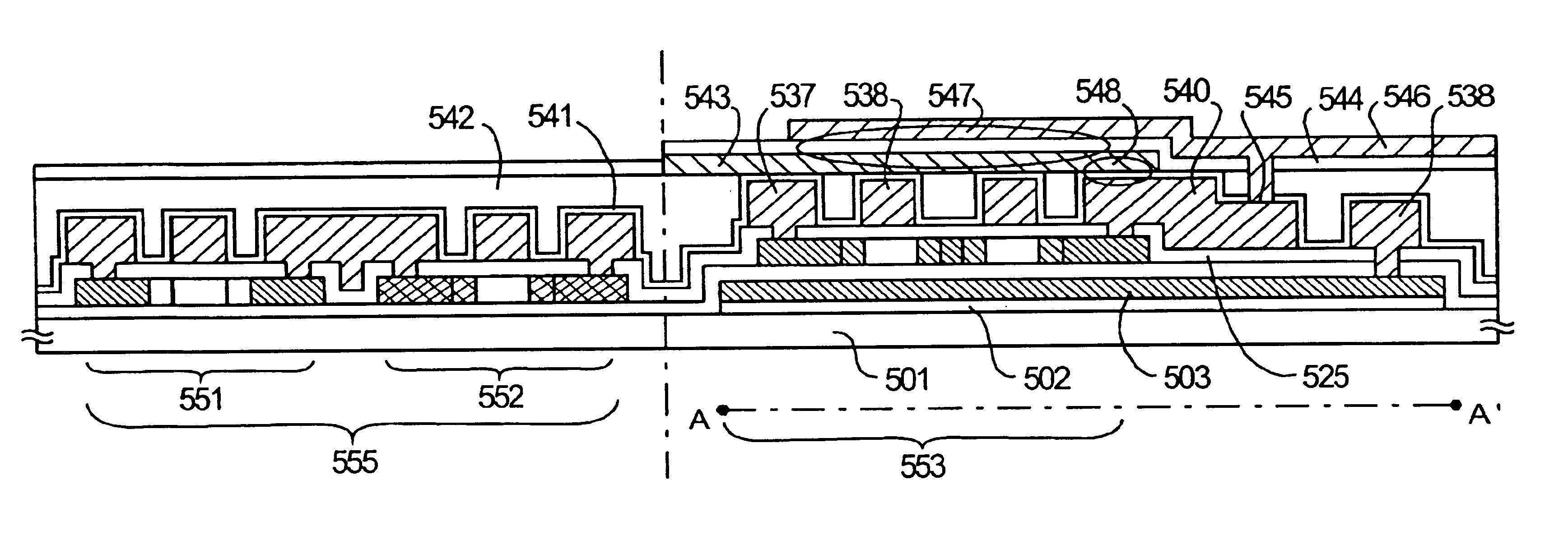
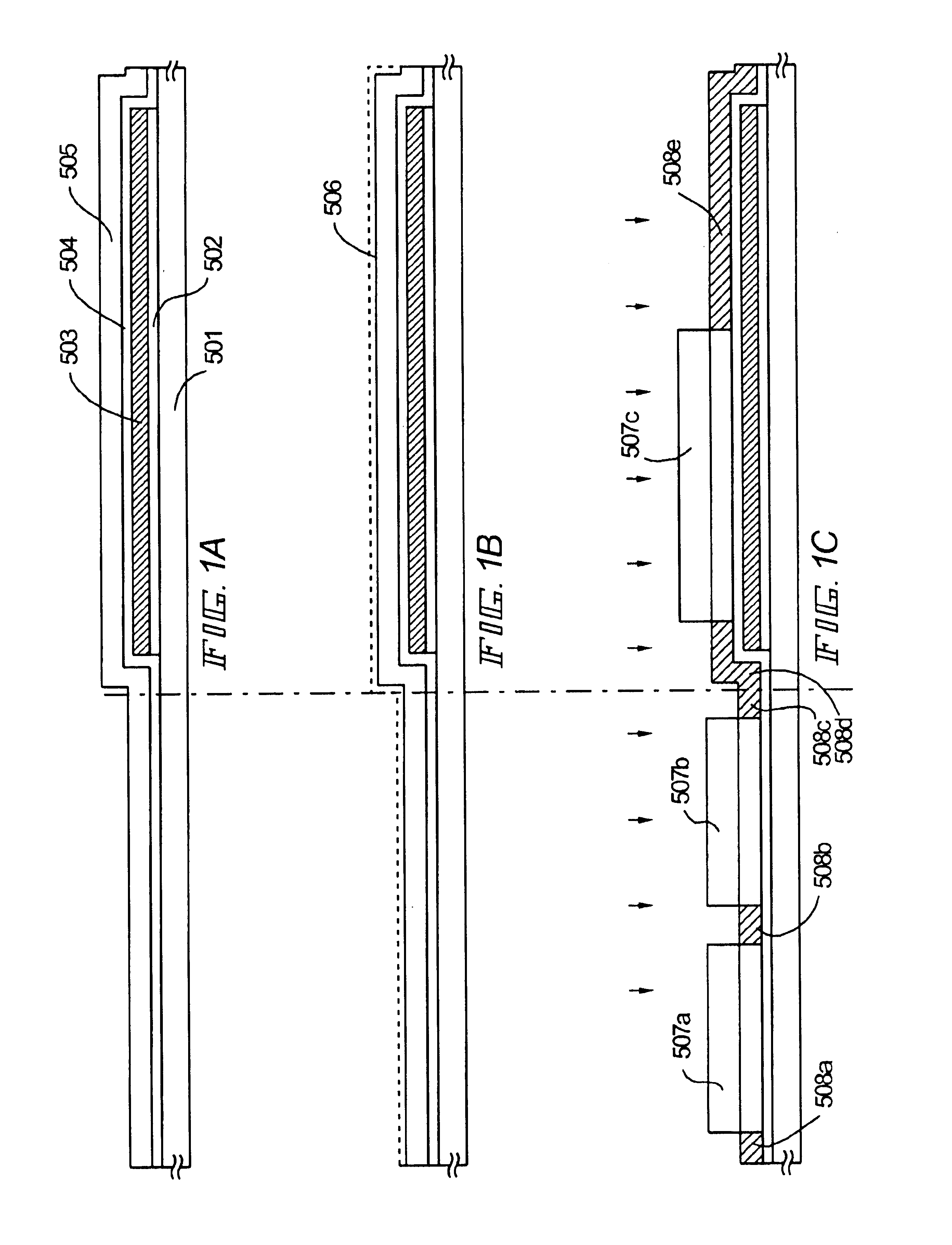
This embodiment explains a method for fabricating an active-matrix substrate, with using FIGS. 1A to 8. In the description, the substrate having a CMOS circuit, a drive circuit, and a pixel region having pixel TFTs and holding capacitances, formed on the same substrate is referred to as an active-matrix substrate for convenience.

First, this embodiment uses a substrate 501 formed of barium borosilicate glass or aluminum borosilicate glass, represented by Coning 7059 glass or 1737 glass. The substrate 501 may use a quartz substrate, a single-crystal silicon substrate or a metal or stainless-steel substrate, having an insulating film formed on a surface. Otherwise, may be used a plastic substrate having a heat resistance to a process temperature in this embodiment. This embodiment uses a quartz glass substrate.

Next, a lower light-shielding film is formed over the quartz substrate 501. First, formed is an underlying film of insulating film, such as a silicon oxide film, a si...

embodiment 2

This embodiment explains a method to fabricate a holding capacitance in a pixel region in a manner different from that of Embodiment 1. Note that the process is the same as the formation of up to the second interlayer insulating film shown in FIG. 4B on Embodiment 1, and hence omittedly explained.

An upper light-shielding film is formed on the second interlayer insulating film. This embodiment uses, in an upper light-shielding film, layers of a film 643a based on titanium and a film 643b based on aluminum. By carrying out anodic oxidation or plasma oxidation on a surface of the upper light-shielding film, anodization is made in a part of the aluminum-based film 643b and titanium-based film 643a to form an aluminum oxide film (alumina film) as an oxide insulating film 644b. The oxide insulating film 644b is used as a dielectric of a holding capacitance. Incidentally, the oxide insulating film obtained by anodizing tantalum (Ta) or titanium (Ti) has a high dielectric constant and hence...

embodiment 3

This embodiment explains a method for manufacturing an active-matrix substrate having TFTs of a GOLD structure formed by the use of the invention. Note that the process is the same as that of Embodiment 1 up to the formation of the conductive film shown in FIG. 3C and hence omittedly explained.

Herein, a photolithography process is used to form a resist mask (not shown) and carry out etching for forming electrodes and interconnections. At this time, the etching process is made such that the low-concentration impurity region in part is overlapped with the gate electrode. In this manner, an interconnection 634 is formed connecting the gate electrode 633, 635, 638, the source interconnection 632. 637, the drain interconnection 636, 640, the n-channel TFT and the p-channel TFT. (FIG. 11A)

Then, by forming up to a pixel electrode 546 according to Embodiment 1, an active-matrix substrate is completed. (FIG. 11B)

In the active-matrix substrate thus formed, because the gate electrode, the sour...


PUM

PropertyMeasurementUnit
thicknessaaaaaaaaaa
thicknessaaaaaaaaaa
thicknessaaaaaaaaaa

Abstract

It is a problem to realize, by a reduced number of processes than that of the conventional, a reliable active-matrix liquid crystal display device having a high opening ratio for high-definition display. The present invention is characterized by: forming a gate electrode and source and drain interconnections in the same process, forming a first insulating film covering the interconnections, forming an upper light-shielding film on the first insulating film, forming a second insulating film on the upper light-shielding film, partially etching the first and second insulating films to form a contact hole reaching the drain interconnection, and forming a pixel electrode on the second insulating film to connect to the drain interconnection. Meanwhile, a holding capacitance is formed by the upper light-shielding film, the second insulating film and the pixel electrode.

Description

BACKGROUND OF THE INVENTION1. Field of the InventionThe present invention relates to a semiconductor device having a circuit structured with thin film transistors (hereinafter, referred to as TFTs) and to a method for manufacturing the same. Particularly, the invention relates to an electro-optical device represented by the liquid crystal display panel and an electronic appliance mounted with such an electro-optical device as a part. Incidentally, in this description, the semiconductor device refers to the devices in general capable of functioning by the utilization of a semiconductor characteristic, i.e. an electro-optical device, a semiconductor circuit and an electronic appliance, in any, are fallen under a semiconductor device.2. Description of the Prior ArtRecently, development has been proceeded for semiconductor devices having TFTs structured by using a thin film (thickness: approximately several to several hundred nm) formed on a substrate having an insulating surface to hav...

Claims


Application Information

Patent Timeline
Patent Type & Authority Patents(United States)
IPC IPC(8): G02F1/1362G02F1/13H01L29/66H01L21/70H01L27/12H01L29/786H01L21/84H01L21/77H01L27/13
CPCG02F1/136209G02F1/136213H01L27/1255H01L29/78633H01L29/78621G02F2201/40H01L29/78645
Inventor ARAO, TATSUYATANADA, YOSHIFUMISHIBATA, HIROSHI
Owner SEMICON ENERGY LAB CO LTD
Why Eureka
Try Eureka