

Chemical treatment of low-k dielectric films
a dielectric film and low-k technology, applied in the direction of semiconductor devices, semiconductor/solid-state device details, electrical apparatus, etc., can solve the problems of etching of the dielectric film itself, damage to the surface of the remaining low-k dielectric film, damage to the exposed surface of the low-k dielectric film
- Summary
- Abstract
- Description
- Claims
- Application Information
AI Technical Summary
Benefits of technology
Problems solved by technology
Method used
Image

Examples
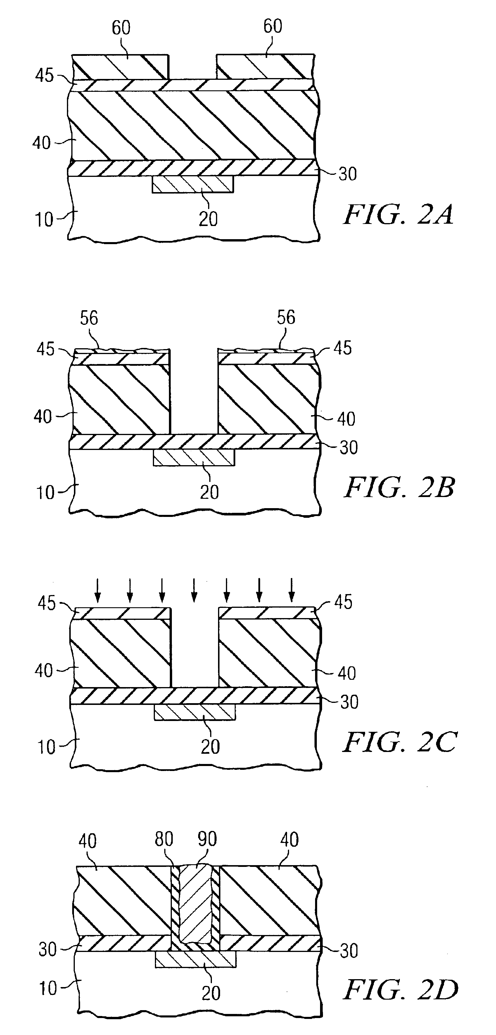
second embodiment
According to the invention, insulator layer 40 is treated with activated hydrogen to repair damage to the film from plasma processes such as the removal of photoresist. The particular conditions of this hydrogen treatment may vary, depending upon the process conditions, and the fluorine-bearing precursor used to provide the chemically reactive fluorine species. Examples of the chemical precursors that may be used in connection with this invention include H2, CH4, other alkanes, and NH3; other precursor compounds may alternatively be used as the hydrogen source, as will be apparent to those skilled in the art having reference to this specification. As discussed above, it is contemplated that either thermal decomposition of the precursor compound, or plasma activation of the hydrogen species may be used, as well as a combination of the two (i.e., plasma enhanced chemical decomposition).
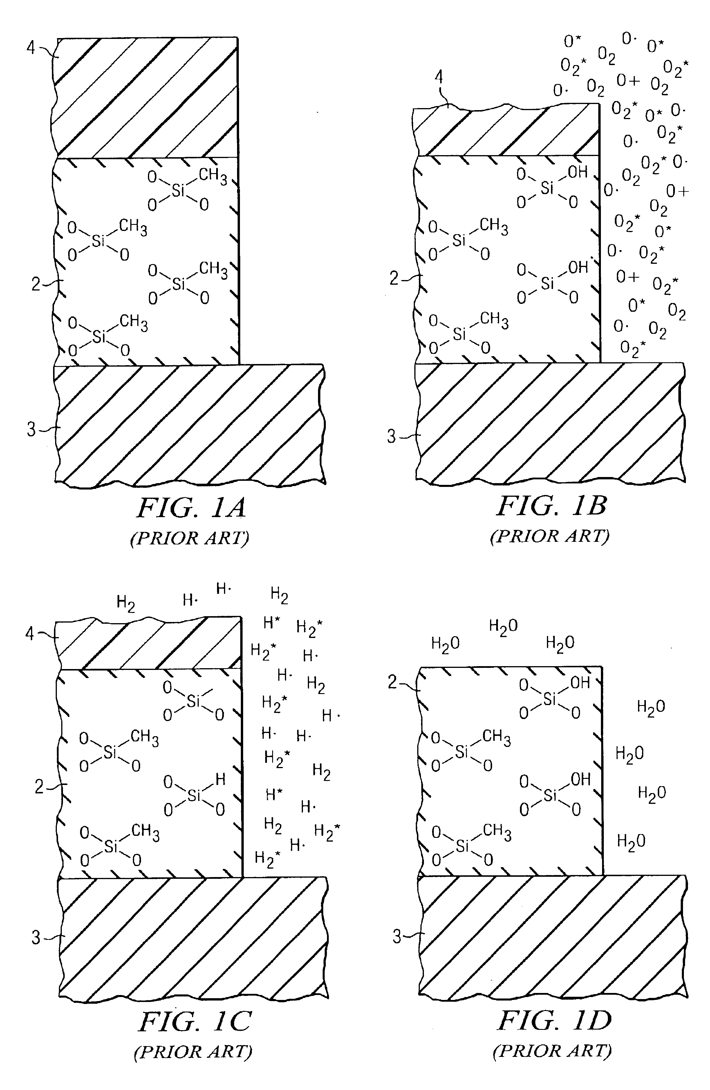
It was mentioned above, relative to FIG. 1c, that hydrogen plasma can be the cause of damage to insu...
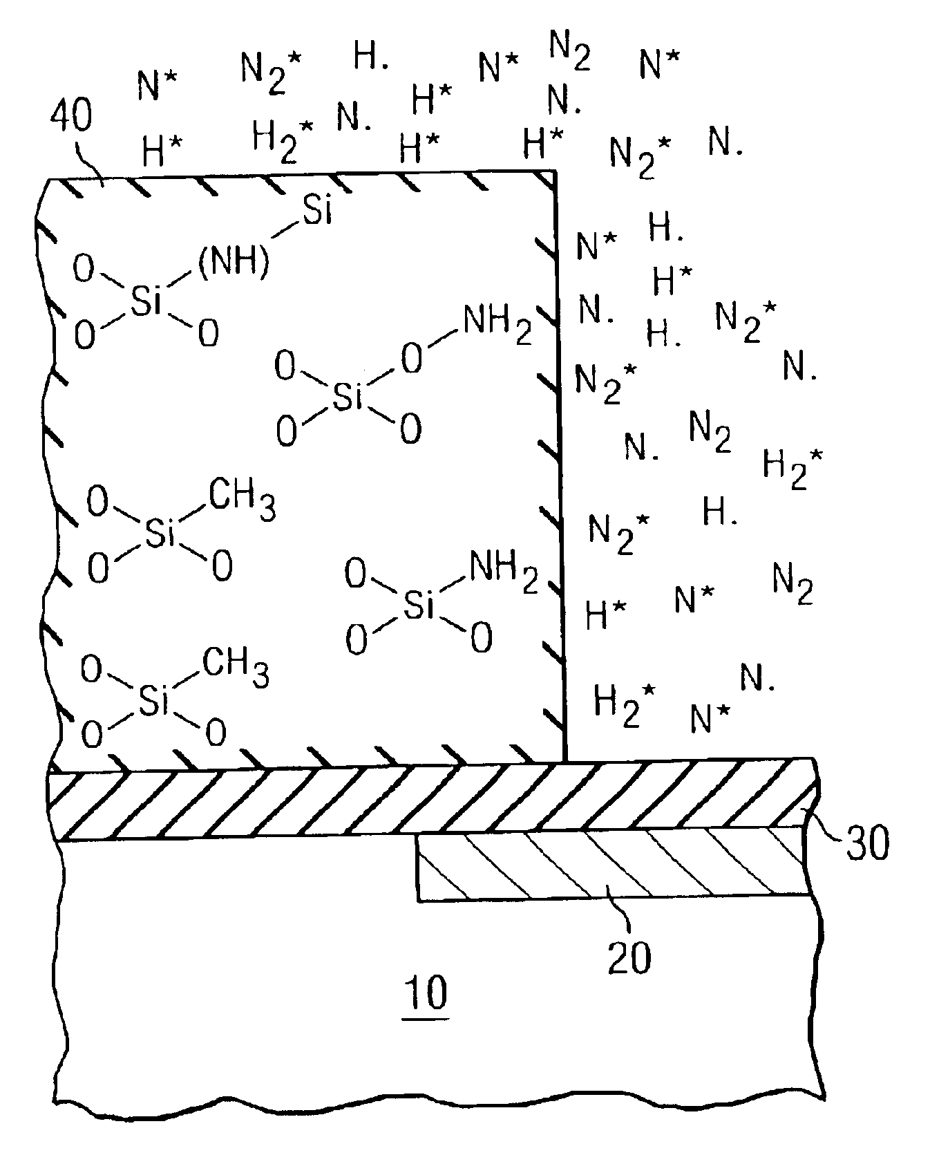
third embodiment
According to the invention, insulator layer 40 is treated with activated nitrogen and hydrogen to repair plasma damage by way of a nitridation reaction. Examples of the chemical precursors that may be used in connection with this embodiment of the invention include NH3 and its related substituted compounds, N2 in combination with CH4 or its related alkane hydrocarbons or in combination with H2; other precursor compounds and combinations may alternatively be used as the nitrogen and hydrogen sources, as will be apparent to those skilled in the art having reference to this specification. As discussed above, it is contemplated that either thermal decomposition of the precursor compounds, or plasma activation of the nitrogen and hydrogen species may be used, as well as a combination of the two (i.e., plasma enhanced chemical decomposition). In either case, the thermal or plasma activation results in atomic, molecular, and ionic species of nitrogen and hydrogen that are capable of reacti...
PUM
 Abstract
Description
Claims
Application Information