System LSI and a cross-bus switch apparatus achieved in a plurality of circuits in which two or more pairs of a source apparatus and a destination apparatus are connected simultaneously and buses are wired without concentration

Inactive Publication Date: 2005-01-11
PANASONIC CORP
View PDF8 Cites 13 Cited by
  • Summary
  • Abstract
  • Description
  • Claims
  • Application Information

AI Technical Summary

Benefits of technology

[0027]It is therefore an object of the present invention to provide a cross-bus switch, a system LSI or the like which can execute data transfers between different source apparatuses and different destination apparatuses simultaneously by two or more transfer requests, and have an improved wiring efficiency without concentration of bus wiring.

Problems solved by technology

There are two types of delays in signal transfer: (1) a delay caused in operation of switching transistors; and (2) a delay caused during signal transfer through wires.
This is because the ratio of the delay in signal transfer through wires to the whole signal transfer delay becomes large as the rule for the processing technique becomes minute.
When such a large number of signal lines gather at one place, the wiring length inevitably becomes large.
This decreases wiring efficiency, increases the signal transfer delay remarkably, and causes the operating frequency to level off.

Method used


Image

  • System LSI and a cross-bus switch apparatus achieved in a plurality of circuits in which two or more pairs of a source apparatus and a destination apparatus are connected simultaneously and buses are wired without concentration
  • System LSI and a cross-bus switch apparatus achieved in a plurality of circuits in which two or more pairs of a source apparatus and a destination apparatus are connected simultaneously and buses are wired without concentration
  • System LSI and a cross-bus switch apparatus achieved in a plurality of circuits in which two or more pairs of a source apparatus and a destination apparatus are connected simultaneously and buses are wired without concentration

Examples


embodiment 1

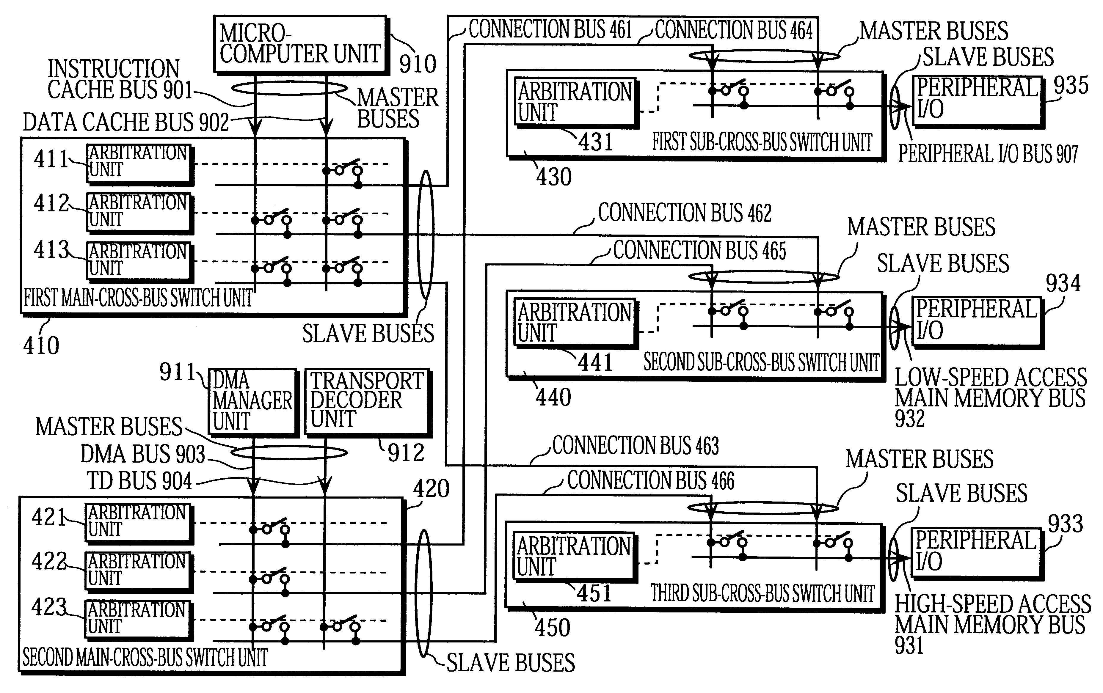
[0089]The cross-bus switch apparatus in Embodiment 1 of the present invention is characterized in that it has two circuits separated from a conventional circuit while the cross-bus switch apparatus has the same function as conventional techniques. More specifically, the TD bus and the other buses connected to the master bus side in the main-cross-bus switch unit are separated into different circuits; buses other than the TD bus are connected as master buses to the sub-cross-bus switch unit; and these cross-bus switch units are connected via a connection bus. The cross-bus switch apparatus of the present embodiment is expected to have excellent wiring efficiency and increased operating frequency.

[0090]

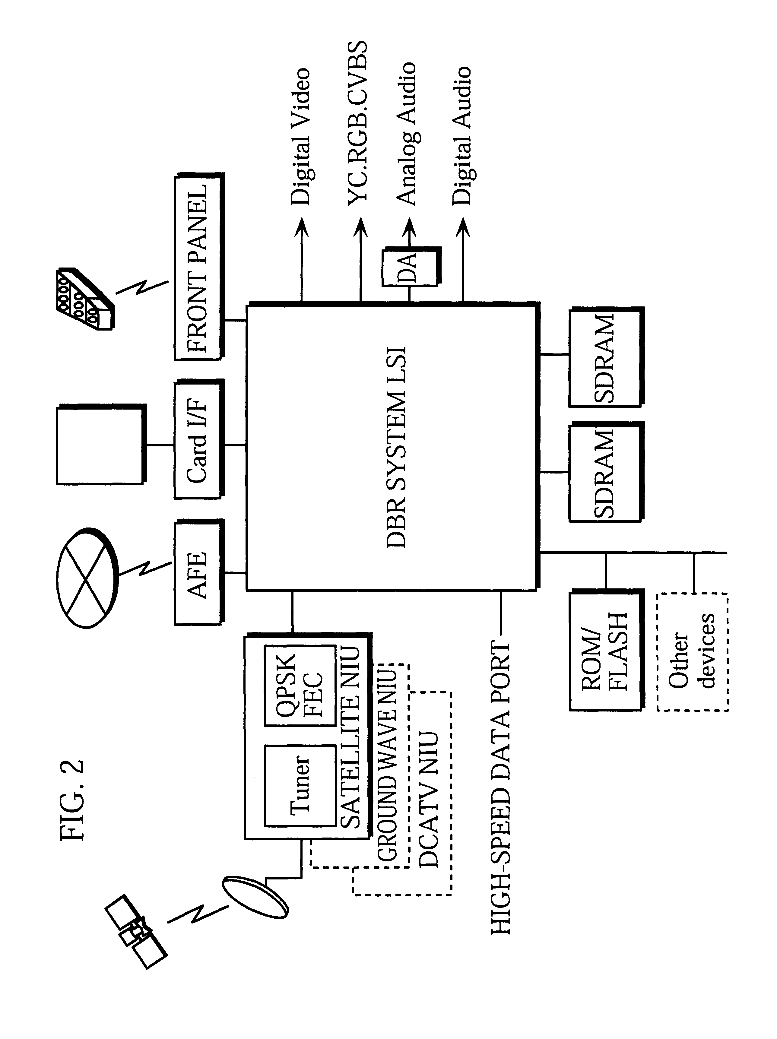
[0091]FIG. 7 shows the construction of the DBR system LSI using the cross-bus switch apparatus in Embodiment 1 of the present invention. The drawing also shows external devices or the like (two “SDRAM”s, a “ROM”, “Other devices”) connected to the DBR system LSI via ports.

[0092]The cross...

embodiment 2

[0129]The cross-bus switch apparatus in Embodiment 2 of the present invention uses an SDRAM as the high-speed access main memory in Embodiment 1. Also, the sub-cross bus switch unit of the present embodiment includes a slave bus corresponding to each bank of the SDRAM so that each bank can be connected to a master bus.

[0130]

[0131]FIG. 11 shows a simplified construction of the cross-bus switch apparatus in Embodiment 2 of the present invention. The drawing also shows units connected to the cross-bus switch apparatus.

[0132]The cross-bus switch apparatus in Embodiment 2 of the present invention includes a main-cross-bus switch unit 320, a sub-cross-bus switch unit 340, a connection bus 360, and an active bank transfer unit 380.

[0133]As shown in FIG. 11, the main-cross-bus switch unit 320 is connected to a set of master buses: the instruction cache bus 901, the data cache bus 902, and the DMA bus 903, and is connected to a set of slave buses: the peripheral I / O bus 907, the low-speed ac...

embodiment 3

[0146]The cross-bus switch apparatus in Embodiment 3 of the present invention is characterized in that source buses connected to the master bus side are grouped into two source bus groups on a substantially even basis, the two source bus groups are connected as master buses to two main-cross-bus switch units, and connection buses as many as destination buses to be connected are connected as slave buses to two main-cross-bus switch units. The same connection buses being slave buses for the two main-cross-bus switch units are connected as master buses to each sub-cross-bus switch unit corresponding to a destination bus, and the destination buses are connected to each sub-cross-bus switch unit as slave buses. This construction enables a circuit to be divided into a plurality of circuits without impairing the function, improving wiring efficiency and increasing operating frequency.

[0147]

[0148]FIG. 12 shows a simplified construction of the cross-bus switch apparatus in Embodiment 3 of th...


PUM


Abstract

A cross-bus switch apparatus which establishes simultaneously two or more pairs of connections between (i) a source bus arbitrarily selected from a plurality of source buses connected to one or more source apparatuses and (ii) a destination bus arbitrarily selected from a plurality of destination buses connected to one or more destination apparatuses. The cross-bus switch apparatus includes: a plurality of cross-bus switch units. The plurality of source buses are grouped into a plurality of source bus groups which are each connected to one of the plurality of cross-bus switch units. The plurality of destination buses are grouped into a plurality of destination bus groups which are each connected to one of the plurality of cross-bus switch units. Each cross-bus switch unit is connected to either (i) a source bus group or a destination bus group, or (ii) a source bus group and a destination bus group.

Description

BACKGROUND OF THE INVENTION[0002](1) Field of the Invention[0003]The present invention relates to a system LSI and a cross-bus apparatus in which two or more pairs of a source apparatus and a destination apparatus, respectively arbitrarily selected from a plurality of apparatuses, are connected simultaneously.[0004](2) Description of the Prior Art[0005]Recently, what is called large system integration (LSI) has become commercially practical. In the system LSI integration, almost all main parts of a system which would have conventionally been achieved as a plurality of LSIs interconnected on a printed board are integrated into a system LSI.[0006]A merit of the system LSI integration is a low cost achieved by its small size. Another merit among others is reduced delays in signal transfer. There are two types of delays in signal transfer: (1) a delay caused in operation of switching transistors; and (2) a delay caused during signal transfer through wires. Of these, the delay in switchi...

Claims


Application Information

Patent Timeline
IPC IPC(8): G06F13/00H03K17/00G06F13/40
CPCG06F13/4031G06F13/4022
Inventor OSAKA, MASATAKASEKIBE, TSUTOMU
Owner PANASONIC CORP
Why Eureka
Try Eureka