Reducing noise effects in circuit boards

a technology of noise effects and circuit boards, applied in the direction of electrical apparatus construction details, printed circuit non-printed electric components association, final product manufacturing, etc., can solve the problem that the smt decoupling capacitor cannot the inability of the smt decoupling capacitor to effectively provide a low-impedance bypass path for switching noise at high frequencies, etc. problem, to achieve the effect of improving the decoupling characteristics

Inactive Publication Date: 2005-01-18
TERADATA US
View PDF14 Cites 23 Cited by
  • Summary
  • Abstract
  • Description
  • Claims
  • Application Information

AI Technical Summary

Problems solved by technology

The number of input / output (I / O) pins that exist on each IC chip can be quite large, which means that a large number of signal wires are needed to carry signals from one IC chip to another component in the system.
With large numbers of IC chips and signal wires (I / O circuits) in a circuit board, switching noise can be a problem during system operation, especially at high frequencies.
One issue associated with connecting decoupling capacitors to reference planes is the relatively high inductance resulting from the combination of the capacitor's package, a via, and the interconnecting structure from the decoupling capacitor to the via.
Nevertheless, because of the increased impedance caused by the inductance of the via, the SMT decoupling capacitor is unable to effectively provide a low-impedance bypass path for switching noise at high frequencies.
In other words, because of a significant impedance introduced by the via inductance into the decoupling path, a capacitor loses its decoupling effectiveness in providing a bypass path for high frequency noise.
However, conventional embedded capacitance techniques are typically associated with relatively low capacitance, which means increased impedance at high frequencies.
Without effective decoupling, switching noise on a circuit board can cause device operation to fail under certain conditions.

Method used


Image

  • Reducing noise effects in circuit boards
  • Reducing noise effects in circuit boards
  • Reducing noise effects in circuit boards

Examples


Embodiment Construction

In the following description, numerous details are set forth to provide an understanding of the present invention. However, it will be understood by those skilled in the art that the present invention may be practiced without these details and that numerous variations or modifications from the described embodiments are possible.

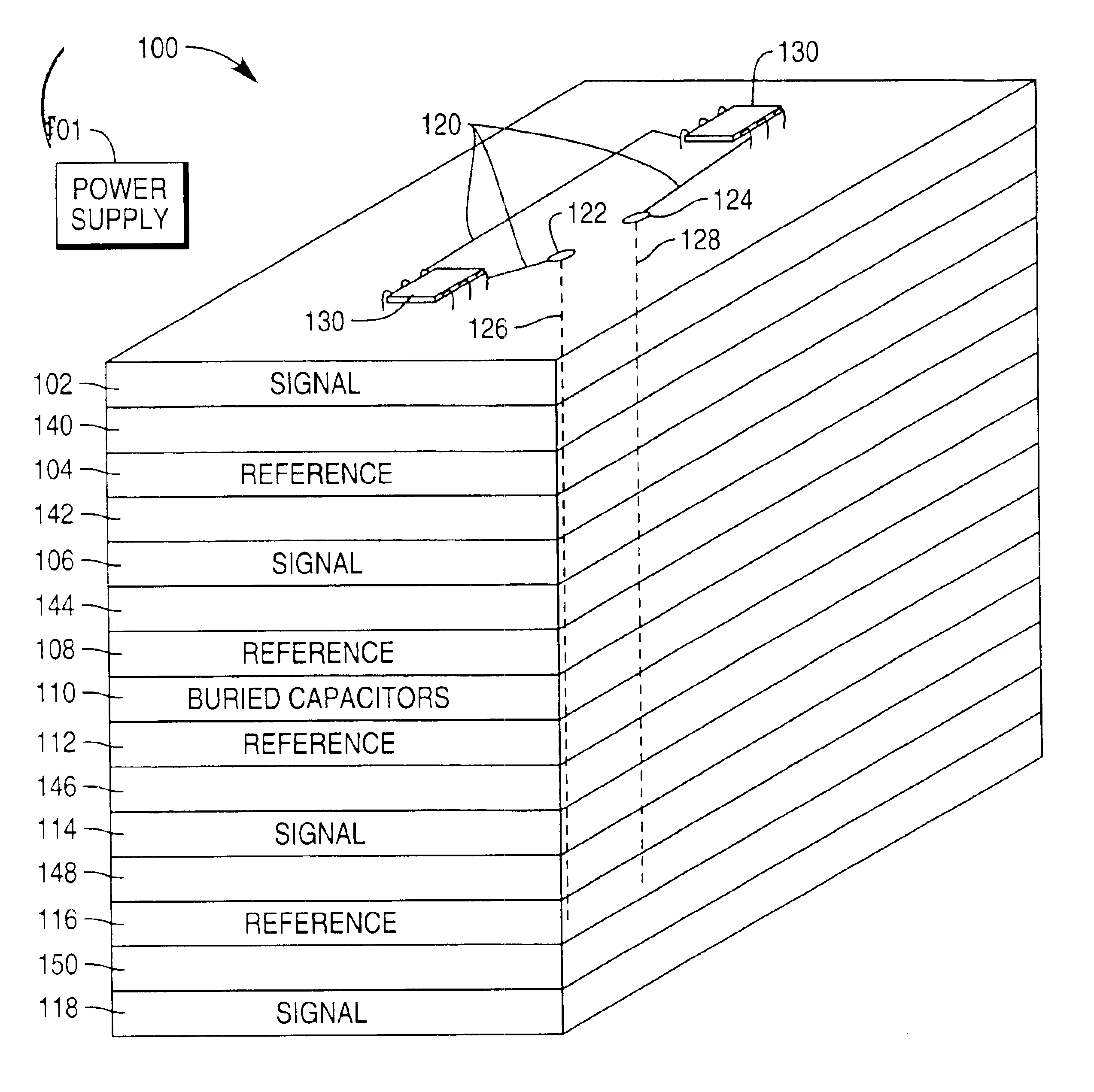
As shown in FIG. 1, an example circuit board 100 includes multiple layers 102, 104, 106, 108, 112, 114, 116, and 118. In other embodiments, a larger or smaller number of layers can be used in the circuit board. As used here, a “circuit board” refers to any structure containing signal wires or conductors (for routing signals) and containing power reference planes (to carry ground and power supply voltages). Examples of a “circuit board” include printed wiring boards (PWBs) and printed circuit boards (PCBs). A “circuit board” also covers any package, such as an integrated circuit (IC) package, that has multiple layers of signal wires or conductors and power ref...


PUM

PropertyMeasurementUnit
voltageaaaaaaaaaa
voltageaaaaaaaaaa
voltageaaaaaaaaaa

Abstract

A circuit board includes an assembly having first and second power reference plane layers, and an insulator layer between the first and second power reference plane layers. Discrete decoupling capacitors are further provided with the assembly. Additional layers are provided above and below the assembly.

Description

BACKGROUNDA circuit board (sometimes referred to as a printed circuit board or a printed wiring board) is the basic building block for interconnecting electronic devices in a system. Electronic devices, usually integrated circuit (IC) devices, are mounted onto the circuit boards using a number of mounting mechanisms, such as by use of connectors or by directly mounting the devices onto a surface of the circuit board. A circuit board also includes the wiring required to interconnect the devices electrically.The number and density of signal lines in a circuit board are continuously increasing due to the increased density of circuits that can be formed on each IC chip. The number of input / output (I / O) pins that exist on each IC chip can be quite large, which means that a large number of signal wires are needed to carry signals from one IC chip to another component in the system. To increase the density of signal wires that can be provided in the circuit board, a circuit board is usuall...

Claims


Application Information

Patent Timeline
Patent Type & Authority Patents(United States)
IPC IPC(8): H05K1/02H05K1/18H05K3/46
CPCH05K1/0231H05K1/185H05K3/4611H05K2201/09309H05K2201/10636Y10T29/49131Y10T29/49165Y10T29/49133Y10T29/49144Y10T29/49155Y10T29/4913Y02P70/50
Inventor FAN, JUNKNIGHTEN, JAMES L.ALEXANDER, ARTHUR R.SMITH, NORMAN W.
Owner TERADATA US
Why Eureka
Try Eureka